TWELITE DIP BLUE (Certification Model: TWE-001 Lite) / TWELITE DIP RED (Certification Model: TWELITE RED) are TWELITE modules in an easy-to-handle DIP format. They feature an ultra-low power and high-performance microcontroller, flash memory, and a high-performance IEEE802.15.4-compliant wireless transceiver.
By connecting power and sensors and storing programs in flash memory or EEPROM, the module can be operated.
Supports SPI, I2C, and UART, allowing connection to various sensors and microcontrollers.
Certified for use in Japan, making it ready for immediate productization.
Features
Compliant with the globally standardized IEEE802.15.4
Proprietary protocol stack “TWELITE NET” available
2.54mm pitch, 28-pin (600mil) DIP IC form factor
Stable long-distance communication enabled by board design maximizing chip performance
Equipped with 32KB RAM and 160KB/512KB flash memory for high-performance communication applications
Standby current is as low as 0.1μA (RAMOFF sleep), contributing to long battery life
Rich I/O including 4 or 6 AD converters, 1 comparator, and 20 GPIOs enables direct sensor connection
Firmware can be modified thanks to onboard flash memory
Firmware development supported by free GNU-based development environment
Secure communication enabled via powerful 128-bit AES encryption
Certified under Japan’s ARIB STD-T66 (technical compliance), allowing use without licensing or additional applications
RoHS compliant, meeting new environmental standards
Specifications
Product Variations
TWELITE DIP BLUE and TWELITE DIP RED come in the variations listed below. Please select the most suitable one for your application.
Sales codes are subject to change. Please refer to our website for the latest codes.
TWELITE Name
Sales Code
Antenna
Remarks
TWELITE DIP BLUE
TWE-L-DI-W
Matchstick Antenna Type
With Pin Headers
TWE-L-DP-W
Without Pin Headers
TWE-L-DI-U
Coaxial Connector Type
With Pin Headers, Antenna Sold Separately
TWE-L-DP-U
Without Pin Headers, Antenna Sold Separately
TWELITE DIP RED
MW-R-DI-W
Matchstick Antenna Type
With Pin Headers
MW-R-DI-W
Without Pin Headers
MW-R-DI-U
Coaxial Connector Type
With Pin Headers, Antenna Sold Separately
MW-R-DI-U
Without Pin Headers, Antenna Sold Separately
Radio Section
TWELITE DIP BLUE
TWELITE DIP RED
Remarks
Communication Method
2.4GHzCompliant with IEEE 802.15.4
2.4GHzCompliant with IEEE 802.15.4
Protocol Stack
TWELITE NET andIEEE 802.15.4 MAC
TWELITE NET andIEEE 802.15.4 MAC
Communication Speed
Up to 250kbps
Up to 250kbps
Modulation Method
O-QPSK, DSSS
O-QPSK, DSSS
Number of Channels
16
16
May vary by country
Transmit Power
2.5dBm
9.19dBm
25℃,3V
Receiver Sensitivity
-95dBm
-96dBm
25℃,3V,typ
Transmit Current
15.3mA
23.3mA
25℃,3V,typ At max output
-
14.0mA
At 3dBm output
Receive Current
17.0mA
14.7mA
25℃,3V,typ
Microcontroller Section
32-bit RISC processor
Variable clock enables optimized power consumption
Fine-grained power control per block (Digital/Analog/RAM/Wireless)
Built-in AES 128-bit encryption circuit and 16-bit random number generator
Interfaces
Qty
Remarks
ADC
4/6
10bit. 4 ports for TWELITE BLUE, 6 ports for TWELITE RED
PWM
4
Timer/PWM
1
5 modes including PWM, Δ∑. 16MHz, 16-bit precision
Pulse Counter
2
Operates in sleep mode. Up to 100kHz, 16-bit
UART
2
16550A compatible
SPIMaster/Slave
1
3 chip selects, up to 16MHz
Comparator
1
2-wire SerialMaster/Slave(I2C, SMBUS compatible)
1
Up to 100kHz or 400kHz, 7/10bit address mode
General-purpose Digital
20
Shared with other I/F
Many pins are shared; availability depends on usage combinations.
Certifications and Regulatory
TWELITE DIP BLUE
TWELITE DIP RED
Certification Model
TWE-001 Lite
TWELITE RED
Technical Conformity Certification Number
007-AB0031
007-AF0062
FCC ID
2AINN-L1
-
IC ID
21544-L1
-
Remarks
RoHS Compliant
RoHS Compliant
*1. When using TWELITE overseas, please check with us early in development due to restrictions on antennas, etc.
*2. Some countries may require labeling of FCC ID or IC ID on TWELITE or products. Contact us if applicable.
Export Notes
The built-in AES 128-bit encryption circuit in TWELITE is subject to export control classification. We will issue a classification document upon request.
Depending on the country, products may not pass customs unless TWELITE has wireless certification. Please inquire for details.
Product Labeling
Product labels, certification numbers, etc., are printed on the device but may change without notice.
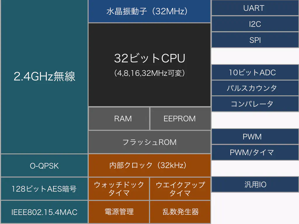
Block Diagram
Block diagram of TWELITE DIP series
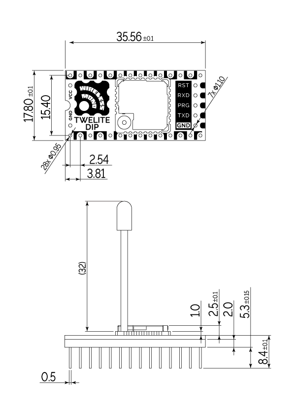
Dimensions
External dimensions of TWE-L-DI-W
Dimensions
Weight
Remarks
35.56mm x 17.8mm x 3.5mm
2.2g
Excluding antenna, connector, and terminals
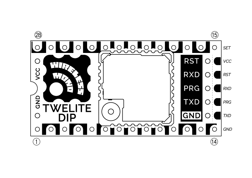
Pin Assignment
Pin Number
Pin Numbers and Assignments
The tail pads are compatible with the 7P interface of TWELITE R2/R3.
When soldering, be careful not to bridge the 5P through-hole next to the pad.
Pin Assignment
#(*1)
IO Name (*2)
Function Assignment (*3)
Alternate Assignment (*4)
Feature Name in “Extremely Simple! Standard App” (*5)
1
GND
GND
2
DIO14
SIF_CLK
TXD1
TXD0
SPISEL1
SCL
3
DIO7
RXD0
PWM3
RX
4
DIO5
RTS0
PWM1
PC1
PWM1
5
DIO18
SPIMOSI
DO1
6
DO0
SPICLK
PWM2(*6)
PWM2
7
DO1
SPIMISO
PWM3(*6)
PWM3
8
DIO19
SPISEL0
DO2
9
DIO4
CTS0
TIM0OUT
PC0
DO3
10
DIO6
TXD0
PWM2
TX
11
DIO8
TIM0CK_GT
PC1
PWM4
PWM4
12
DIO9
TIM0CAP
32KTALIN
RXD1
DO4
13
DIO10
TIM0OUT
32KTALOUT
M1
14
GND
GND
15
DIO12
PWM2
CTS0
DI1
16
DIO13
PWM3
RTS0
DI2
17
DIO11
PWM1
TXD1
DI3
18
DIO16
COMP1P
SIF_CLK
DI4
19
DIO15
SIF_D
RXD1
RXD0
SPISEL2
SDA
20
DIO17
COMP1M
PWM4
SIF_D
BPS
21
RESETN
RESETN
RST
22
ADC1
AI1
23
DIO0
SPISEL1
ADC3
AI2
24
ADC2
VREF
AI3
25
DIO1
SPISEL2
ADC4
PC0
AI4
26
DIO2
ADC5(*7)
TIM0CK_GT
M2
27
DIO3
ADC6(*7)
TIM0CAP
M3
28
VCC
VCC
VCC
(*1) Pin number. The number and assignment of pins differ from TWELITE (SMD version). Usually, use the IO Name to specify pins.
(*2) Pin definition name. This is used in semiconductor datasheets and TWELITE app development; our technical support also refers to pins by their IO Name.
(*3) Each pin can be used as simple I/O or analog input, but you can assign other functions via API initialization. This table lists typical functions.
(*4) By initializing via API, you can move functions to alternate assignment pins. This table lists typical alternate functions.
(*5) Pin names specific to the “Extremely Simple! Standard App” (App_Twelite). These are similar to IO Names; take care not to confuse them.
(*6) PWM2,3 can be assigned to DO0,1 by releasing the assignment of DIO6,7 or DIO12,13.
(*7) ADC5 and ADC6 are available only on TWELITE RED.
Function Overview
Signal Name
Function
PC
Pulse Counter
SPICLK
SPI Clock
SPISEL
SPI Select Output
SPIMISO
SPI Controller Input (SDI)
SPIMOSI
SPI Controller Output (SDO)
TIM0CK_GT
Timer Clock, Gate Input
TIM0CAP
Timer Capture Input
TIM0OUT
Timer PWM Output
32KTALIN
Crystal Input
32KTALOUT
Crystal Output
VREF
Reference Voltage
COMP1M
Comparator + Input
COMP1P
Comparator - Input
SIF_D
2-wire Serial Data
SIF_CLK
2-wire Serial Clock
RXD
UART RX
TXD
UART TX
RTS
UART RTS
CTS
UART CTS
PWM
Pulse Width Modulation Output
Handling of Special Pins
DO0 (Function: SPICLK)
This pin is used as an output.
Applying voltage from external sources
(even with some output impedance) has been reported to cause the TWE module to not enter programming mode. When connecting LEDs or transistors, the pin may enter an intermediate state upon startup or wake from sleep, potentially causing malfunction. We recommend configuring the external circuit so that it is always pulled up to Vcc.
DO1 (Function: SPIMISO)
This pin is often used as an output, but at module power-up or reset, it behaves as an input. If the voltage is judged as Low at that time, the module will start in programming mode. Pay attention to the
voltage level at startup
on this pin.
DIO0 (Function: ADC3), DIO1 (Function: ADC4)
These pins are shared with analog input. In firmware,
the internal pull-up must be disabled when reading AD values
.
ADC2
ADC2 can be used as a reference voltage input. Software implementation is required to use this. Note that
there is no pin to output the reference voltage.
GND
It is recommended to connect both pins 1 and 14 to GND, but operation is possible with either unconnected. No significant change in wireless performance has been observed if one is left unconnected.
Absolute Maximum Ratings
Min
Max
Power Supply (VCC)
-0.3
3.6
V
Analog IO (VREF/ADC)
-0.3
VCC+0.3
V
Digital IO
-0.3
VCC+0.3
V
Characteristics
Recommended Operating Conditions
Symbol
Condition
min
typ
max
Power Supply Voltage
VCC
2.0
3.0
3.6
V
Startup Voltage
Vboot
2.05
V
Operating Temperature
TOPR
No condensation
TWELITE DIP BLUE
-40
25
105(*1) 90(*2)
℃
TWELITE DIP RED
-30
25
90
Operating Humidity
HOPR
No condensation
85
%RH
Values are based on semiconductor datasheet. *1 Max operating temperature of TWE-L-WX *2 Max operating temperature of TWE-L-U
DC Characteristics
Symbol
Condition
min
typ
max
Current Consumption
ICC
Sleep(RAMOFF, no timer)
TWELITE DIP BLUE
0.1
uA
TWELITE DIP RED
0.1
uA
Sleep(with timer)
TWELITE DIP BLUE
1.5
uA
TWELITE DIP RED
1.5
uA
Transmit (CPU doze)
TWELITE DIP BLUE
15.3
mA
TWELITE DIP RED
23.3
mA
TWELITE DIP RED(at 3dBm output)
14.0
mA
Receive (CPU doze)
TWELITE DIP BLUE
17.0
mA
TWELITE DIP RED
14.7
mA
Transmit Power
Pout
TWELITE DIP BLUE
+0.5
2.5
dBm
TWELITE DIP RED
9.14
dBm
Receiver Sensitivity
TWELITE DIP BLUE
-95
dBm
TWELITE DIP RED
-96
dBm
Values are based on semiconductor datasheet.
I/O Characteristics
Symbol
Condition
min
typ
max
Internal Pull-up on DIO
40
50
60
kΩ
DIO High Input
VIH
VCCx0.7
VCC
V
DIO Low Input
VIL
-0.3
VCCx0.27
V
DIO Input Hysteresis
200
310
400
mV
DIO High Output
VOH
TWELITE DIP BLUE
VCCx0.8
VCC
V
TWELITE DIP RED
VCC-0.4
DIO Low Output
VOL
0
0.4
V
DIO Load, Sink Current
IOL
VCC 2.7~3.6V
4
mA
VCC 2.2~2.7V
3
mA
VCC 2.0~2.2V
2.5
mA
Values are based on semiconductor datasheet.
ADC Characteristics
Symbol
Condition
min
typ
max
Reference Voltage
VREF
1.198
1.235
1.260
V
ADC Resolution
10
Bits
ADC Integral Nonlinearity
±1.6, ±1.8
LSB
ADC Differential Nonlinearity
-0.5
0.5
LSB
ADC Offset Error
0~VREF
-10
mV
0~2VREF
-20
ADC Gain Error
TWELITE DIP BLUE0~VREF
+10
mV
TWELITE DIP BLUE0~2VREF
+20
TWELITE DIP RED0~VREF
-10
TWELITE DIP RED0~2VREF
-20
ADC Clock
0.25,0.5, 1.0
MHz
ADC Input Range
0.04
VREF2xVREF
V
Values are based on semiconductor datasheet.
Precautions for Use
Storage
Avoid high temperature and humidity. Use the product within six months of delivery.
General Notes
Please be sure to evaluate and verify the product in your actual usage environment.
For applications requiring high reliability or involving human safety, please consult with your distributor in advance.
Revision History
Version
Revision Date
Revision Details
2.0.1
2024/11/12
Corrected unit mislabeling for current consumption
TWELITE DIP BLUE (Certification Model: TWE-001 Lite) / TWELITE DIP RED (Certification Model: TWELITE RED) are TWELITE modules in an easy-to-handle DIP format. They feature an ultra-low power and high-performance microcontroller, flash memory, and a high-performance IEEE802.15.4-compliant wireless transceiver.
By connecting power and sensors and storing programs in flash memory or EEPROM, the module can be operated.
Supports SPI, I2C, and UART, allowing connection to various sensors and microcontrollers.
Certified for use in Japan, making it ready for immediate productization.
Features
Compliant with the global standard IEEE802.15.4
Supports proprietary protocol stack “TWELITE NET”
28-pin (600mil) DIP IC form factor with 2.54mm pitch
PCB design maximizes chip performance enabling stable long-range communication
Equipped with 32KB RAM and 160KB/512KB flash memory, capable of running high-performance communication applications
Ultra-low standby current of 0.1μA (RAMOFF sleep mode) extends battery life
Rich I/O including 4 or 6 AD converters, 1 comparator, and 20 general-purpose I/Os allow direct connection to sensors
Built-in flash memory allows firmware updates
Firmware can be developed using free GNU and Eclipse-based environments
Robust 128-bit AES encryption ensures security
Certified under Japan’s ARIB STD-T66, no license or application required for domestic use
RoHS compliant, meets new environmental standards
Specifications
Product Model Numbers
TWELITE DIP BLUE and TWELITE DIP RED are available in the variations shown in the table below. Please select the most appropriate one for your application.
Since sales codes may change from time to time, please refer to our website for the latest information.
Common Name
Sales Code
Antenna
Remarks
TWELITE DIP BLUE
TWE-L-DI-W
Stick Antenna Type
Pin header mounted
TWE-L-DP-W
Pin header not mounted
TWE-L-DI-P
2D Stick Antenna Type
Pin header mounted
TWE-L-DP-P
Pin header not mounted
TWE-L-DI-U
Coaxial Connector Type
Pin header mounted, antenna not included
TWE-L-DP-U
Pin header not mounted, antenna not included
TWELITE DIP RED
MW-R-DI-W
Stick Antenna Type
Pin header mounted
MW-R-DI-W
Pin header not mounted
MW-R-DI-U
Coaxial Connector Type
Pin header mounted, antenna not included
MW-R-DI-U
Pin header not mounted, antenna not included
Wireless Section
TWELITE DIP BLUE
TWELITE DIP RED
Remarks
Communication Method
2.4GHzIEEE 802.15.4 compliant
2.4GHzIEEE 802.15.4 compliant
Protocol Stack
TWELITE NET andIEEE 802.15.4 MAC
TWELITE NET andIEEE 802.15.4 MAC
Data Rate
Up to 250kbps
Up to 250kbps
Modulation
O-QPSK, DSSS
O-QPSK, DSSS
Number of Channels
16
16
May differ by country
Transmit Power
2.5dBm
9.19dBm
25℃, 3V
Receiver Sensitivity
-95dBm
-96dBm
25℃, 3V, typ
Transmit Current
15.3mA
23.3mA
25℃, 3V, typ, max output
-
14.0mA
At 3dBm output
Receive Current
17.0mA
14.7mA
25℃, 3V, typ
Microcontroller Section
32-bit RISC processor
Variable clock for optimized power consumption
RAM: 32kBytes
EEPROM: 4kBytes
Flash memory: TWELITE DIP BLUE 160kBytes / TWELITE DIP RED 512kBytes
Watchdog timer, brown-out detection
Fine-grained power control for each block (digital/analog/RAM/wireless)
Built-in AES 128bit encryption circuit, 16bit random number generator
Many are shared pins and may not be available depending on the combination used.
Antenna
TWE-*-W0 comes with a stick antenna, W7 comes with a question-mark type antenna.
There is also a board antenna that can be mounted on the PCB. If you wish to use it, we will provide drawings, so please contact us via the inquiry form on our website.
For TWE-*-U external antenna versions, please refer to our website.
If you wish to use antennas other than the supported types with TWELITE, separate radio certification is required. Please contact us.
Certifications
TWELITE DIP BLUE
TWELITE DIP RED
Certification Model
TWE-001 Lite
TWELITE RED
Technical Conformity Certification Number
007-AB0031
007-AF0062
FCC ID
2AINN-L1
-
IC ID
21544-L1
-
Remarks
RoHS compliant
RoHS compliant
※1. When using TWELITE overseas, there may be various restrictions such as permitted antennas. Please consult us in the early stage of development.
※2. Depending on the country, it may be necessary to display FCC ID, IC ID, etc. on TWELITE or the product. If you think this applies, please contact us.
Notes on Export
The built-in AES 128bit encryption circuit in TWELITE is subject to export control judgment. When exporting, we will issue an export control certificate, so please contact us.
In some countries, customs clearance may not be possible unless TWELITE has obtained radio certification in the exporting country. Please inquire about regulations for each country.
Product Labeling
The product bears product logos, certification numbers, etc., but these may change without notice.
Block Diagram
Dimensions
Sales Code
Dimensions
Weight
Remarks
TWE-L-DI-W/TWE-L-DP-W
35.7mm x 17.7mm x 3.5mm
2.2g
Excluding antenna, connector, and terminals
TWE-L-DI-U/TWE-L-DP-U
35.7mm x 17.7mm x 3.5mm
2.2g
TWE-L-DI-P/TWE-L-DP-P
47.5mm x 17.7mm x 3.5mm
2.7g
MW-R-DI-W/ MW-R -DP-W
35.7mm x 17.7mm x 3.5mm
2.2g
MW-R-DI-U/ MW-R-DP-U
35.7mm x 17.7mm x 3.5mm
2.2g
DXF data for TWE-L-DI-W outline is available for download on our website.
Pin Assignment
Pin Number
Pin Mapping
#(*1)
IO Name (*2)
Function Assignment (*3)
Alternative Assignment (*4)
Extremely Simple! Standard App Function Name (*5)
1
GND
GND
2
DIO14
SIF_CLK
TXD1
TXD0
SPISEL1
SCL
3
DIO7
RXD0
PWM3
RX
4
DIO5
RTS0
PWM1
PC1
PWM1
5
DIO18
SPIMOSI
DO1
6
DO0
SPICLK
PWM2(*6)
PWM2
7
DO1
SPIMISO
PWM3(*6)
PWM3
8
DIO19
SPISEL0
DO2
9
DIO4
CTS0
TIM0OUT
PC0
DO3
10
DIO6
TXD0
PWM2
TX
11
DIO8
TIM0CK_GT
PC1
PWM4
PWM4
12
DIO9
TIM0CAP
32KTALIN
RXD1
DO4
13
DIO10
TIM0OUT
32KTALOUT
M1
14
GND
GND
15
DIO12
PWM2
CTS0
DI1
16
DIO13
PWM3
RTS0
DI2
17
DIO11
PWM1
TXD1
DI3
18
DIO16
COMP1P
SIF_CLK
DI4
19
DIO15
SIF_D
RXD1
RXD0
SPISEL2
SDA
20
DIO17
COMP1M
PWM4
SIF_D
BPS
21
RESETN
RESETN
RST
22
ADC1
AI1
23
DIO0
SPISEL1
ADC3
AI2
24
ADC2
VREF
AI3
25
DIO1
SPISEL2
ADC4
PC0
AI4
26
DIO2
ADC5(*7)
TIM0CK_GT
M2
27
DIO3
ADC6(*7)
TIM0CAP
M3
28
VCC
VCC
VCC
*1. Pin number. Different from TWELITE (SMD version) in numbering and assignment. Use IO Name to identify pins.
*2. IO Name is the pin’s defined name, used in semiconductor datasheets and TWELITE app development. This is also the default naming used in our technical support.
*3. Each pin can be used for general input/output or analog input, but can also be initialized via API to assign alternative functions. This column lists representative assignments.
*4. Functions listed here are available when the pin is initialized via API for alternate use.
*5. Function names specific to the “Extremely Simple! Standard App” (App_Twelite). These may resemble IO names but are distinct.
*6. PWM2 and PWM3 can be reassigned from DIO6,7 or DIO12,13 to DO0,1.
*7. ADC5 and ADC6 are available only on TWELITE RED.
Function Description
Signal Name
Function
PC
Pulse Counter
SPICLK
SPI Master Clock
SPISEL
SPI Select Output
SPIMISO
SPI Master Input
SPIMOSI
SPI Master Output
TIM0CK_GT
Timer Clock, Gate Input
TIM0CAP
Timer Capture Input
TIM0OUT
Timer PWM Output
32KTALIN
Crystal Input
32KTALOUT
Crystal Output
VREF
Reference Voltage
COMP1M
Comparator + Input
COMP1P
Comparator - Input
SIF_D
2-wire Serial Data
SIF_CLK
2-wire Serial Clock
RXD
UART RX
TXD
UART TX
RTS
UART RTS
CTS
UART CTS
PWM
Pulse Width Modulation Output
Handling of Special Pins
DO0 (Function Name: SPICLK)
This pin is used as an output pin.
Applying voltage externally
(even with some output impedance) has been reported to prevent the TWE module from entering program mode. When connecting LEDs or transistors, the pin may be in an intermediate state at startup or when waking from sleep, causing abnormal operation. It is recommended to always use an external circuit that pulls up to Vcc.
DO1 (Function Name: SPIMISO)
This pin is often used as an output pin, but at module power-on or reset it behaves as an input. If a low voltage is detected at that time, the module starts in program mode. Please pay attention to the
voltage at startup
on this pin.
These pins are shared with analog input. In firmware,
internal pull-up must be disabled when reading AD values
.
ADC2
ADC2 can be used as an input for reference voltage. Software implementation is required to use this. Note,
there is no pin that outputs the reference voltage.
GND
It is recommended to connect both pins 1 and 14 to GND, but it is also possible to operate with one unconnected. No significant change in wireless performance has been observed even if either is left unconnected.
Absolute Maximum Ratings
Min
Max
Power Supply (VCC)
-0.3
3.6
V
Analog IO (VREF/ADC)
-0.3
VCC+0.3
V
Digital IO
-0.3
VCC+0.3
V
Characteristics
Recommended Operating Conditions
Symbol
Condition
min
typ
max
Supply Voltage
VCC
2.0
3.0
3.6
V
Startup Voltage
Vboot
2.05
V
Operating Temperature
TOPR
No condensation
TWELITE DIP BLUE
-40
25
105(*1) 90(*2)
℃
TWELITE DIP RED
-30
25
90
Operating Humidity
HOPR
No condensation
85
%RH
Values based on semiconductor datasheet. *1 Maximum operating temperature for TWE-L-WX/W0/W7 *2 Maximum operating temperature for TWE-L-U
DC Characteristics
Symbol
Condition
min
typ
max
Current Consumption
ICC
Sleep(RAMOFF no timer)
TWELITE DIP BLUE
0.1
uA
TWELITE DIP RED
0.1
uA
Sleep(with timer)
TWELITE DIP BLUE
1.5
uA
TWELITE DIP RED
1.5
uA
Tx (CPU doze)
TWELITE DIP BLUE
15.3
mA
TWELITE DIP RED
23.3
uA
TWELITE DIP RED(at 3dBm output)
14.0
uA
Rx (CPU doze)
TWELITE DIP BLUE
17.0
mA
TWELITE DIP RED
14.7
mA
Transmit Power
Pout
TWELITE DIP BLUE
+0.5
2.5
dBm
TWELITE DIP RED
9.14
dBm
Receiver Sensitivity
TWELITE DIP BLUE
-95
dBm
TWELITE DIP RED
-96
dBm
Values based on semiconductor datasheet.
I/O Characteristics
Symbol
Condition
min
typ
max
DIO Internal Pull-Up
40
50
60
kΩ
DIO High-Level Input
VIH
VCCx0.7
VCC
V
DIO Low-Level Input
VIL
-0.3
VCCx0.27
V
DIO Input Hysteresis
200
310
400
mV
DIO High-Level Output
VOH
TWELITE DIP BLUE
VCCx0.8
VCC
V
TWELITE DIP RED
VCC-0.4
DIO Low-Level Output
VOL
0
0.4
V
DIO Drive/Sink Current
IOL
VCC 2.7~3.6V
4
mA
VCC 2.2~2.7V
3
mA
VCC 2.0~2.2V
2.5
mA
Values based on semiconductor datasheet.
ADC Characteristics
Symbol
Condition
min
typ
max
Reference Voltage
VREF
1.198
1.235
1.260
V
ADC Resolution
10
Bits
ADC Integral Non-Linearity
±1.6, ±1.8
LSB
ADC Differential Non-Linearity
-0.5
0.5
LSB
ADC Offset Error
0~VREF
-10
mV
0~2VREF
-20
ADC Gain Error
TWELITE DIP BLUE0~VREF
+10
mV
TWELITE DIP BLUE0~2VREF
+20
TWELITE DIP RED0~VREF
-10
TWELITE DIP RED0~2VREF
-20
ADC Clock
0.25,0.5, 1.0
MHz
ADC Input Range
0.04
VREF2xVREF
V
Values based on semiconductor datasheet.
Precautions for Use
Storage
Store in a cool, dry place. Use the product within six months of delivery.
General Notes
Please always evaluate and verify the product in your actual usage environment.
For applications requiring high reliability or involving human life, please consult with your distributor in advance.