TWELITE Wireless Microcontroller Datasheet
Features
- Compliant with the global IEEE802.15.4 standard
- Supports our proprietary protocol stack “TWELITE NET”
- Ultra-compact module (13.97 × 13.97 × 2.5 mm)
- PCB design maximizes chip performance for stable long-range communication
- Equipped with 32KB RAM and 160KB/512KB flash memory, enabling high-performance communication applications
- Extremely low standby current of 0.1μA (RAMOFF sleep), extending battery life
- Rich I/O including 4 or 6 ADCs, 1 comparator, and 20 general-purpose I/O ports for direct sensor connection
- On-board flash memory allows firmware updates
- Firmware development supported by free GNU and Eclipse-based environments
- Robust 128-bit AES encryption ensures security
- Certified under Japan’s ARIB STD-T66 (Technical Conformity), usable without additional license or application
- RoHS compliant, meeting new environmental standards
Specifications
Product Variants
TWELITE BLUE and TWELITE RED are available in the variations shown below. Please select the most suitable model for your application.
Sales codes may change over time. Please refer to our website for the latest sales codes.
| Common Name | Sales Code | Antenna Terminal | Notes |
|---|---|---|---|
| TWELITE BLUE | TWE-L-WX | Wire antenna terminal type | Antenna not included (reel only) |
| TWE-L-U | Coaxial antenna type | Antenna not included | |
| TWELITE RED | MW-R-WX | Wire antenna terminal type | Antenna not included |
| MW-R-U | Coaxial antenna type | Antenna not included |
Wireless Section
| TWELITEBLUE | TWELITERED | Notes | |
|---|---|---|---|
| Communication Method | 2.4GHzIEEE 802.15.4 compliant | 2.4GHzIEEE 802.15.4 compliant | |
| Protocol Stack | TWELITE NET andIEEE 802.15.4 MAC | TWELITE NET andIEEE 802.15.4 MAC | |
| Data Rate | Up to 250kbps | Up to 250kbps | |
| Modulation | O-QPSK, DSSS | O-QPSK, DSSS | |
| Number of Channels | 16 | 16 | May vary by country |
| TX Output Power | 2.5dBm | 9.19dBm | 25°C, 3V |
| RX Sensitivity | -95dBm | -96dBm | 25°C, 3V, typ |
| TX Current | 15.3mA | 23.3mA | 25°C, 3V, typ at max output |
| 14.0mA | At 3dBm output | ||
| RX Current | 17.0mA | 14.7mA | 25°C, 3V, typ |
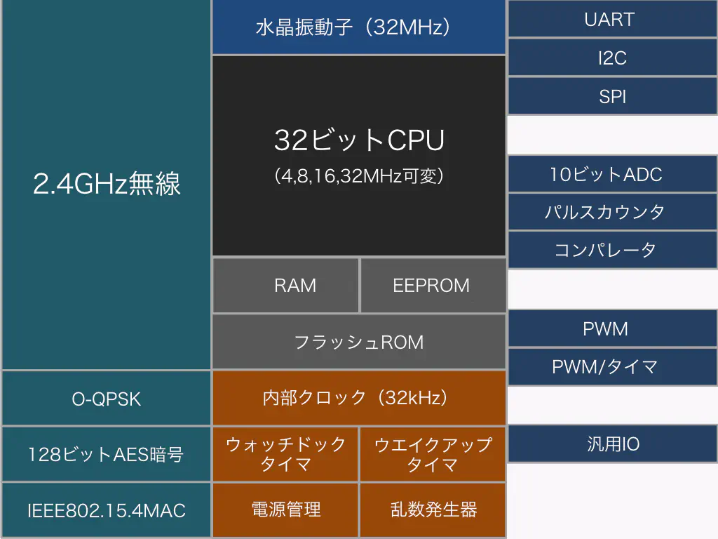
Microcontroller Section
- 32-bit RISC processor
- Variable clock for power optimization
- RAM: 32kBytes
- EEPROM: 4kBytes
- Flash memory: 160kBytes (TWELITE BLUE) / 512kBytes (TWELITE RED)
- Watchdog timer, brown-out detection
- Fine-grained power control for each block (digital/analog/RAM/wireless)
- Built-in AES 128-bit encryption circuit and 16-bit random number generator
Interfaces
| Qty | Notes | |
|---|---|---|
| ADC | 4/6 | 10-bit. 4 ports for TWELITE BLUE, 6 ports for TWELITE RED |
| PWM | 4 | |
| Timer/PWM | 1 | 5 modes including PWM, Δ∑. 16MHz, 16-bit resolution |
| Pulse Counter | 2 | Operates in sleep mode. Max 100kHz, 16-bit |
| UART | 2 | 16550A compatible |
| SPIMaster/Slave | 1 | 3 chip selects, up to 16MHz |
| Comparator | 1 | |
| 2-wire SerialMaster/Slave(I2C, SMBUS compatible) | 1 | Up to 100kHz or 400kHz, 7/10-bit address modes |
| General-purpose Digital | 20 | Shared with other interfaces |
- Many pins are shared; some combinations may not be available simultaneously.
Certifications and Compliance
| TWELITE BLUE | TWELITE RED | |
|---|---|---|
| Certification Model | TWE-001 Lite | TWELITE RED |
| Technical Conformity Number | 007-AB0031 | 007-AF0062 |
| FCC ID | 2AINN-L1 | - |
| IC ID | 21544-L1 | - |
| Notes | RoHS compliant | RoHS compliant |
※1. When using TWELITE outside Japan, there may be restrictions on antennas and other components. Please consult us at the early stage of your development.
※2. Depending on the country, it may be necessary to display the FCC ID or IC ID on TWELITE or your product. If applicable, please contact us.
Export Precautions
- The built-in AES 128-bit encryption circuit in TWELITE is subject to export control. We will issue an export control statement as needed; please contact us when exporting.
- In some countries, customs clearance may not be possible unless TWELITE has obtained local radio certification. Please inquire about regulations for each export destination.
Product Labeling
The product is marked with a logo, certification numbers, etc., which are subject to change without notice.
Block Diagram
External Dimensions
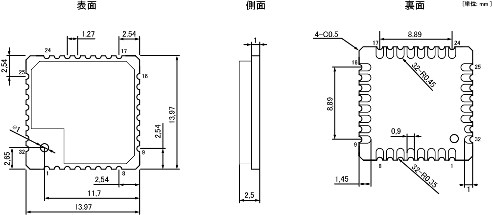
Dimensions: 13.97 × 13.97 × 2.5 mm Weight: 0.93 g
DXF data for TWELITE BLUE/TWELITE RED outlines is available for download from our website.
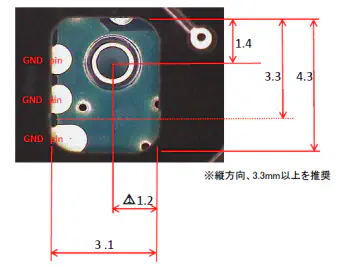
Recommended Pad Dimensions

- The mating PCB contacting the module’s underside must not have silkscreen or through-holes.
- When soldering a wire antenna (such as a matchstick antenna), provide a rectangular hole in the mating PCB and solder from the underside of the module. (See Chapter 7 for details.)
- Use a metal mask thickness in the range of t=0.12–0.15mm. Depending on the mask and reflow conditions, solder fillets may not form on one side of the module’s half-through-holes.
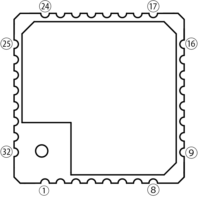
Antenna Mounting Opening
When mounting TWELITE on your custom PCB, it is efficient to provide an opening for connecting a wire antenna (matchstick antenna) and solder from the underside.
This drawing shows an example of such an opening.
In this example, pins 29, 30, 31, and 32 (NC, GND, GND, GND) are left unconnected to allow for a larger opening.
Note: Connecting GND pins 28, 30–32 on the SMD version is recommended, but operation without connection is also possible. No significant change in wireless performance has been observed even if left unconnected.
Pin Assignment
Pin Numbers
Pin Assignment
| # (Note 1) | IO Name (Note 2) | Function Assignment (Note 3) | Alternate Assignment (Note 4) | Super Easy! Standard App Function Name (Note 5) | ||||
|---|---|---|---|---|---|---|---|---|
| 1 | DO0 | SPICLK | PWM2(※6) | PWM2 | ||||
| 2 | DO1 | SPIMISO | PWM3(※6) | PWM3 | ||||
| 3 | DIO18 | SPIMOSI | DO1 | |||||
| 4 | DIO19 | SPISEL0 | DO2 | |||||
| 5 | VCC | VCC | VCC | |||||
| 6 | DIO4 | CTS0 | TIM0OUT | PC0 | DO3 | |||
| 7 | DIO5 | RTS0 | PWM1 | PC1 | PWM1 | |||
| 8 | DIO6 | TXD0 | PWM2 | TX | ||||
| 9 | DIO7 | RXD0 | PWM3 | RX | ||||
| 10 | DIO8 | TIM0CK_GT | PC1 | PWM4 | PWM4 | |||
| 11 | DIO9 | TIM0CAP | 32KTALIN | RXD1 | DO4 | |||
| 12 | DIO10 | TIM0OUT | 32KTALOUT | M1 | ||||
| 13 | DIO12 | PWM2 | CTS0 | DI1 | ||||
| 14 | DIO14 | SIF_CLK | TXD1 | TXD0 | SPISEL1 | SCL | ||
| 15 | DIO13 | PWM3 | RTS0 | DI2 | ||||
| 16 | DIO11 | PWM1 | TXD1 | DI3 | ||||
| 17 | DIO15 | SIF_D | RXD1 | RXD0 | SPISEL2 | SDA | ||
| 18 | DIO16 | COMP1P | SIF_CLk | DI4 | ||||
| 19 | DIO17 | COMP1M | PWM4 | SIF_D | BPS | |||
| 20 | GND | GND | ||||||
| 21 | RESETN | RESETN | RST | |||||
| 22 | ADC2 | VREF | AI3 | |||||
| 23 | ADC1 | AI1 | ||||||
| 24 | DIO0 | SPISEL1 | ADC3 | AI2 | ||||
| 25 | DIO1 | SPISEL2 | ADC4 | PC0 | AI4 | |||
| 26 | DIO2 | ADC5(※7) | TIM0CK_GT | M2 | ||||
| 27 | DIO3 | ADC6(※7) | TIM0CAP | M3 | ||||
| 28 | GND | GND | GND | |||||
| 29 | NC | RF | N/A | |||||
| 30 | GND | GND | GND | |||||
| 31 | GND | GND | GND | |||||
| 32 | GND | GND | GND |
Note 1. Pin number. Note that the number and assignment may differ from TWELITE DIP. IO name is usually used to identify pins. Note 2. IO name. This is used in semiconductor datasheets, TWELITE app development, and technical support. Note 3. Each pin can be used as simple I/O or analog input, but can also be initialized for other functions via API. The table lists typical functions. Note 4. Alternate functions assignable via API. The table lists typical alternate functions. Note 5. Pin names used by the “Super Easy! Standard App (App_Twelite)”. These are similar to IO names but take care to avoid confusion. Note 6. PWM2,3 can be assigned to DO0,1 by releasing DIO6,7 or DIO12,13 assignments. Note 7. ADC5,6 are available only on TWELITE RED.
Function Reference
| Signal Name | Function |
|---|---|
| PC | Pulse Counter |
| SPICLK | SPI Master Clock |
| SPISEL | SPI Select Output |
| SPIMISO | SPI Master Input |
| SPIMOSI | SPI Master Output |
| TIM0CK_GT | Timer Clock, Gate Input |
| TIM0CAP | Timer Capture Input |
| TIM0OUT | Timer PWM Output |
| 32KTALIN | Crystal Input |
| 32KTALOUT | Crystal Output |
| VREF | Reference Voltage |
| COMP1M | Comparator + Input |
| COMP1P | Comparator - Input |
| SIF_D | 2-wire Serial Data |
| SIF_CLK | 2-wire Serial Clock |
| RXD | UART RX |
| TXD | UART TX |
| RTS | UART RTS |
| CTS | UART CTS |
| PWM | Pulse Width Modulation Output |
Special Pin Handling
DO0 (Function: SPICLK)
This pin is used as an output.
If an external voltage is applied
(even with some output impedance), there have been reports that the TWE module may fail to enter programming mode.
When connecting LEDs or transistors, the pin may enter an intermediate state at startup or wakeup from sleep, possibly causing malfunction. Always use an external circuit that pulls up to Vcc.
DO1 (Function: SPIMISO)
This pin is typically used as an output, but at power-on or reset, it behaves as an input. If a low level is detected at this time, the module boots in programming mode. Pay attention to the voltage at startup on this pin.
DIO0 (Function: ADC3), DIO1 (Function: ADC4)
These pins are shared with analog input. In firmware, the internal pull-up must be disabled when reading AD values .
ADC2
ADC2 can be used as a reference voltage input. Software implementation is required. There is no pin for outputting the reference voltage.
GND
Connecting GND pins 28, 30–32 on the SMD version is recommended, but operation without connection is possible. No significant change in wireless performance has been observed even if left unconnected.
Absolute Maximum Ratings
| Min | Max | ||
|---|---|---|---|
| Power Supply (VCC) | -0.3 | 3.6 | V |
| Analog IO (VREF/ADC) | -0.3 | VCC+0.3 | V |
| Digital IO | -0.3 | VCC+0.3 | V |
Characteristics
Recommended Operating Conditions
| Symbol | Condition | min | typ | max | ||||
|---|---|---|---|---|---|---|---|---|
| Power Supply Voltage | VCC | 2.0 | 3.0 | 3.6 | V | |||
| Startup Voltage | Vboot | 2.05 | V | |||||
| Operating Temperature | TOPR | No condensation | TWELITE BLUE | -40 | 25 | 105(Note 1) 90(Note 2) | °C | |
| TWELITE RED | -30 | 25 | 90 | |||||
| Operating Humidity | HOPR | No condensation | 85 | %RH |
*Values are based on semiconductor datasheets.
Note 1: Maximum operating temperature for TWE-L-WX/W0/W7
Note 2: Maximum operating temperature for TWE-L-U
DC Characteristics
| Symbol | Condition | min | typ | max | |||
|---|---|---|---|---|---|---|---|
| Current Consumption | ICC | Sleep (RAMOFF, no timer) | TWELITE BLUE | 0.1 | uA | ||
| TWELITE RED | 0.1 | uA | |||||
| Sleep (with timer) | TWELITE BLUE | 1.5 | uA | ||||
| TWELITE RED | 1.5 | uA | |||||
| Tx (CPU doze) | TWELITE BLUE | 15.3 | mA | ||||
| TWELITE RED | 23.3 | mA | |||||
| TWELITE RED(at 3dBm output) | 14.0 | mA | |||||
| Rx (CPU doze) | TWELITE BLUE | 17.0 | mA | ||||
| TWELITE RED | 14.7 | mA | |||||
| TX Output Power | Pout | TWELITE BLUE | +0.5 | 2.5 | dBm | ||
| TWELITE RED | 9.14 | dBm | |||||
| RX Sensitivity | TWELITE BLUE | -95 | dBm | ||||
| TWELITE RED | -96 | dBm |
*Values are based on semiconductor datasheets.
I/O Characteristics
| Symbol | Condition | min | typ | max | ||
|---|---|---|---|---|---|---|
| DIO Internal Pull-up | 40 | 50 | 60 | kΩ | ||
| DIO Hi Input | VIH | VCCx0.7 | VCC | V | ||
| DIO Lo Input | VIL | -0.3 | VCCx0.27 | V | ||
| DIO Input Hysteresis | 200 | 310 | 400 | mV | ||
| DIO Hi Output | VOH | TWELITE BLUE | VCCx0.8 | VCC | V | |
| TWELITE RED | VCC-0.4 | |||||
| DIO Lo Output | VOL | 0 | 0.4 | V | ||
| DIO Sink Current | IOL | VCC 2.7–3.6V | 4 | mA | ||
| VCC 2.2–2.7V | 3 | mA | ||||
| VCC 2.0–2.2V | 2.5 | mA |
*Values are based on semiconductor datasheets.
ADC Characteristics
| Symbol | Condition | min | typ | max | ||
|---|---|---|---|---|---|---|
| Reference Voltage | VREF | 1.198 | 1.235 | 1.260 | V | |
| ADC Resolution | 10 | Bits | ||||
| ADC Integral Nonlinearity | ±1.6, ±1.8 | LSB | ||||
| ADC Differential Nonlinearity | -0.5 | 0.5 | LSB | |||
| ADC Offset Error | 0–VREF | -10 | mV | |||
| 0–2VREF | -20 | |||||
| ADC Gain Error | TWELITE BLUE0–VREF | +10 | mV | |||
| TWELITE BLUE0–2VREF | +20 | |||||
| TWELITE RED0–VREF | -10 | |||||
| TWELITE RED0–2VREF | -20 | |||||
| ADC Clock | 0.25,0.5, 1.0 | MHz | ||||
| ADC Input Range | 0.04 | VREF2xVREF | V |
*Values are based on semiconductor datasheets.
Reel Specifications
Taping Dimensions
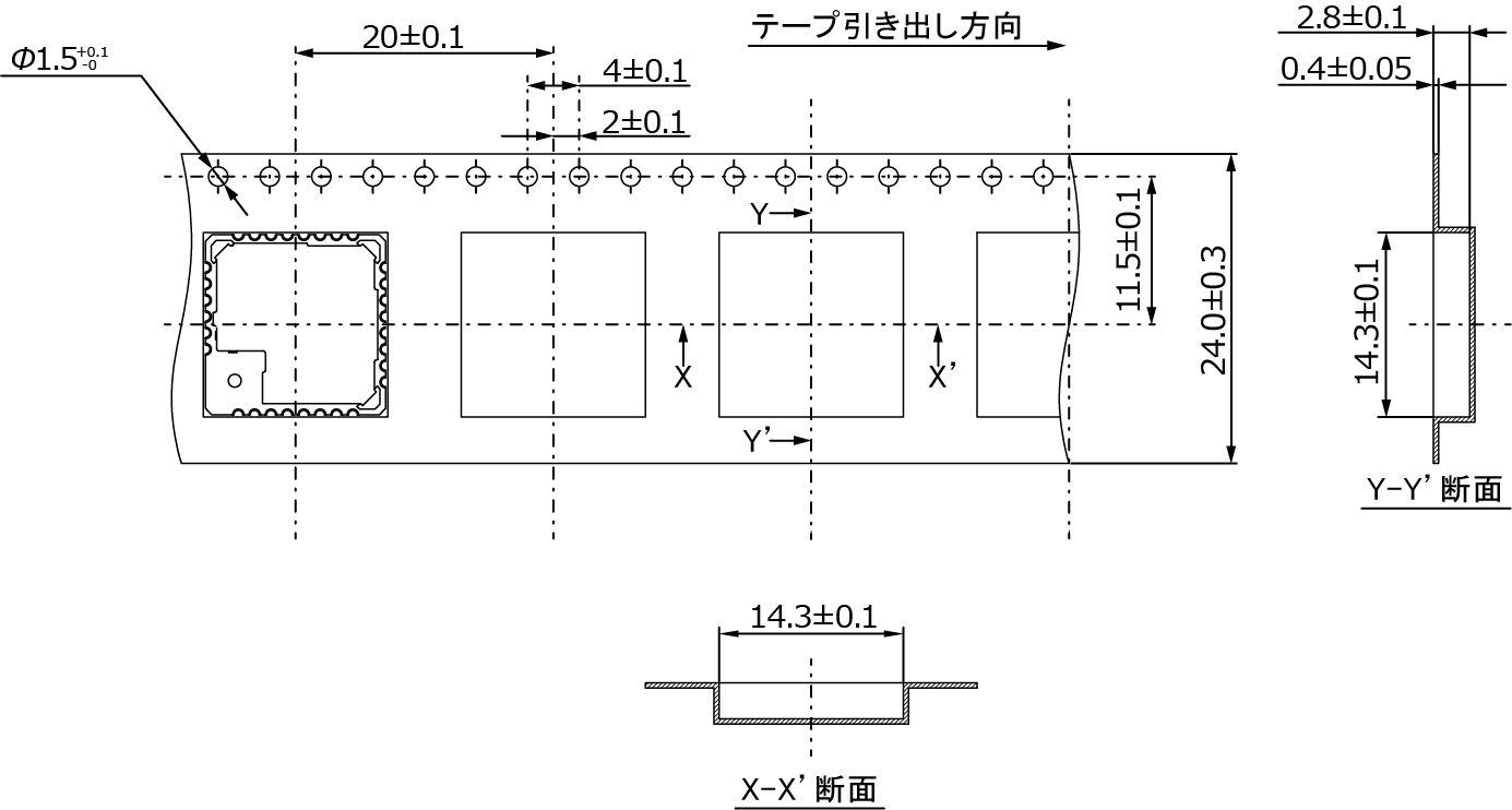
Reel Dimensions

Maximum Module Packaging Quantity
| Reel/Inner Box | Quantity/Reel | Outer Box | Quantity |
|---|---|---|---|
| 1 | 1000 | 1 | 1000 |
Reflow Conditions
Recommended Reflow Profile
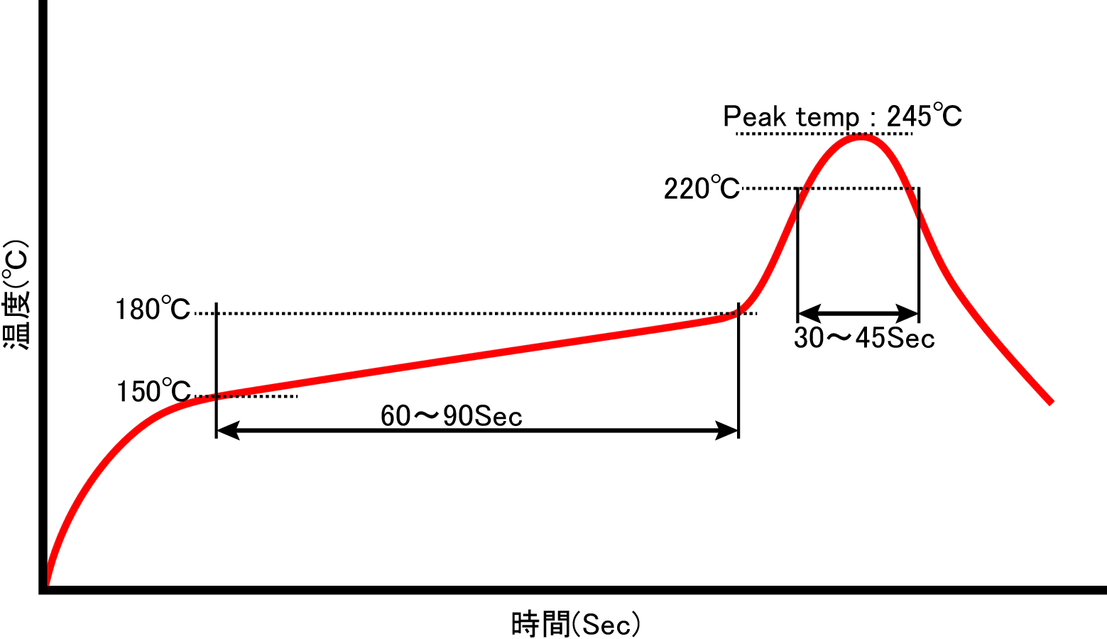
Reflow profile
| Preheating | Main Heating | Peak Temp | Number of Reflows |
|---|---|---|---|
| 150 | 220°C/30~45sec | 245°C | 1 time |
- Temperature conditions: One reflow within the recommended temperature profile above.
- Soldering should be performed by reflow soldering as a general rule.
- We have confirmed no issues under the above profile, but please verify solderability under your own manufacturing conditions.
Board Mounting Precautions
- Only one reflow process is allowed under our recommended conditions. Note that solder inside the module will re-melt during reflow. Reflow soldering is the principle method.
- The product absorbs moisture if left in the natural environment. Mount using reflow within 72 hours after opening.
- When storing below the above humidity, ensure proper anti-static measures.
- If more than 72 hours have passed after opening, bake under the following conditions before use:
- Do not bake reels directly. Transfer to trays, etc., before baking.
- Baking conditions: 90°C, 48 hours, up to 1 time.
- Please note that multiple lot numbers may be mixed in the same package.
- Solder fillets are not required on the soldered parts of components mounted on this product.
- This product is intended for mounting on glass epoxy PCBs. If mounting on other materials (e.g., ceramics), evaluate thoroughly before use.
- Some internal components are highly sensitive to static electricity. Take adequate ESD precautions.
- If stress is applied to the shield case, it may detach. Handle with care.
- For hand soldering, follow these conditions: below 350°C, within 3 seconds (surface temperature must not exceed 150°C).
Precautions for Use
Factory Default Application
At the time of shipment (as of this datasheet’s publication), TWELITE is programmed with the “Super Easy! Standard App” firmware. This firmware is intended for production testing during manufacturing. We cannot disclose information about the firmware version or contents programmed on TWELITE, even upon request. In the future, the presence or type of pre-installed firmware may be changed without notice. Please write the required application to TWELITE during your own manufacturing process.
Storage
Store in a cool, dry place. Use the product within six months of delivery.
General Notes
Always evaluate and verify our products in your actual usage environment.
If you intend to use this product in applications requiring high reliability or involving human life, please consult your distributor in advance.
Revision History
| Version | Date | Revision Details |
|---|---|---|
| 4.0.2 | 2024/11/12 | Corrected current unit error |
| 4.0.1 | 2024/07/12 | Applied sales code changes; antenna column removed |
| 4.0.0 | 2024/02/27 | Migrated to new website |
| 3.0.4 | 2019/1/31 | Added “Factory Default Application” section |
| 3.0.3 | 2018/11/05 | Corrected section number error in Chapter 8 |
| 3.0.2 | 2018/3/7 | Corrected pin function name error in App table |
| 3.0.1 | 2017/9/1 | Corrected TWELITE RED sleep current value |
| 3.0.0 | 2017/8/1 | Initial version |