Introduction
TWELITE® is a compact, low-power, high-performance wireless module.
Equipped with an Arm® Cortex®-M4 core, it supports medium-range wireless communication compliant with IEEE802.15.4 and short-range communication compliant with ISO/IEC 14443.
Certified for radio use in Japan, it enables rapid product development for wireless systems.
Features
- Ultra-compact body package (13.97mm × 13.97mm × 2.5mm)
- Medium-range wireless communication compliant with the global standard IEEE802.15.4
- PCB design that maximizes chip performance and ensures stable communication over long distances
- Our proprietary simple protocol stack “TWELITE NET”
- Short-range wireless communication with NFC readers compliant with ISO/IEC 14443
- Widely used Arm Cortex-M4 architecture
- Excellent power-saving performance with standby current as low as 350nA, contributing to longer battery life
- Equipped with 152KB SRAM and 640KB flash memory to support advanced communication application software
- Six-channel 12-bit ADC and 22 general-purpose digital I/O ports to connect various sensors
- Ten channels of PWM output usable for LEDs and actuators
- Newly added 32-bit real-time clock
- Firmware development environment based on the freely available GNU Arm Embedded Toolchain
- Strong AES encryption: 128bit / 192bit / 256bit
- Certified under Japan’s ARIB STD-T66 construction design certification (technical conformity)
Product Variants
The TWELITE Wireless Module (GOLD Series) comes in the following variations. Please select according to your application.
| Product Name | Model No. | Antenna Terminal | Remarks |
|---|---|---|---|
| TWELITE | MW-G-W | Wire antenna terminal(through-hole) | Antenna sold separately |
| MW-G-U | Coaxial antenna terminal(U.FL/IPEX) | Antenna sold separately | |
| TWELITE DIP | MW-G-DIP-P | PCB antenna | |
| MW-G-DIP-U | Coaxial antenna terminal(U.FL/IPEX) | Antenna sold separatelyMain body: MW-G-W |
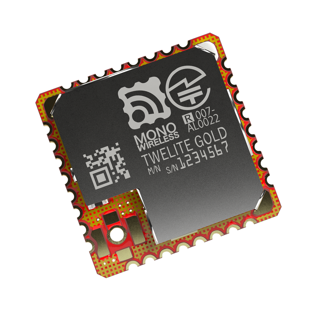
MW-G-W Appearance
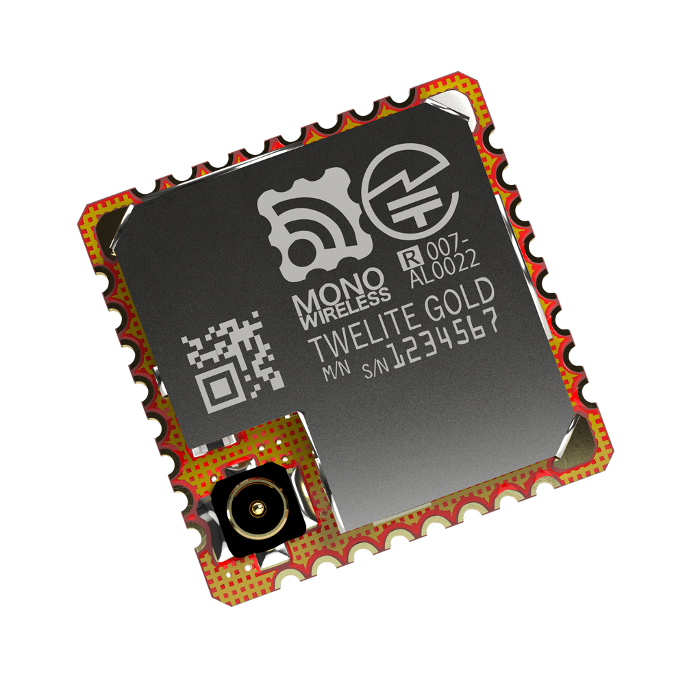
MW-G-U Appearance
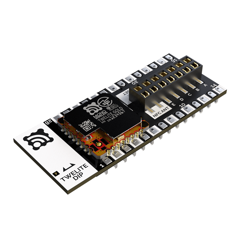
MW-G-DIP-P Appearance
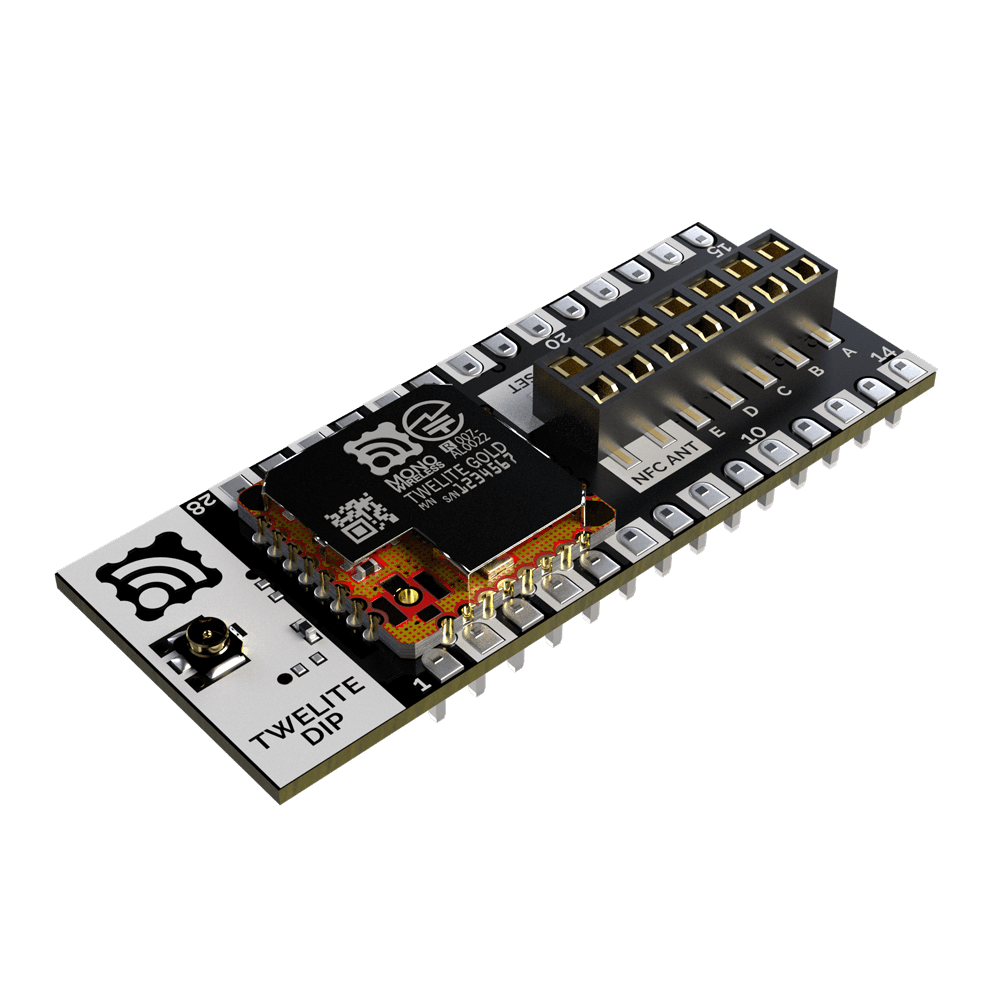
MW-G-DIP-U Appearance
In the following documentation, references related to MW-G-W/U are marked as SMD , those related to MW-G-DIP-P/U as DIP , and those applicable to all as ALL .
Functions
ALL- 32-bit Arm Cortex-M4 processor
- Operating clock: 32MHz (variable between 12MHz and 48MHz to optimize power consumption)
- SRAM: 152KB
- Flash memory: 640KB
- EEPROM: 2KB (mounted on internal NFC chip)
- Watchdog timer, brown-out detection
- Power control for each block (Digital/Analog/SRAM/Wireless)
- AES encryption circuit: 128bit / 192bit / 256bit
- 6x ADC (12-bit)
- 10x PWM
- 2x Timer (32-bit)
- 1x Comparator
- 2x UART
- 2x SPI (with 3 chip selects)
- 2x I2C
- 22x Digital IO
- 1x Quad SPI
- 1x RTC (32-bit)
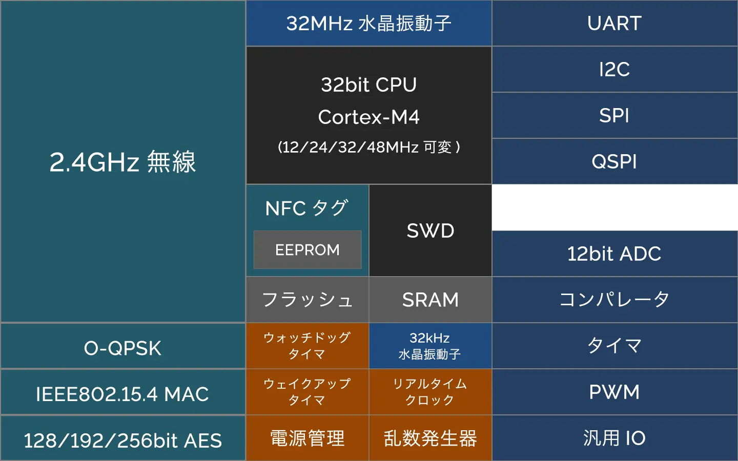
Block Diagram of TWELITE (GOLD Series)
2.4GHz Wireless
ALL| Item | TWELITE (GOLD Series) | Remarks |
|---|---|---|
| Communication | 2.4GHz IEEE 802.15.4 | |
| Protocol | TWELITE NET and IEEE 802.15.4 MAC | |
| Data Rate | 250kbps | |
| Modulation | O-QPSK, DSSS | |
| Channels | 16 | Varies depending on country |
| Max TX Power | 9.14dBm | 25°C, 3V, typical |
| RX Sensitivity | -99.7dBm | 25°C, 3V, typical |
Antenna
ALLFor a list of compatible antennas, refer to our product information.
SMDA board antenna that can be mounted on the PCB (MW-A-P1934) is also available. See Board antenna (MW-A-P1934).
Certification
ALL| TWELITE (GOLD Series) | |
|---|---|
| Certification Model Name | TWELITE GOLD |
| Technical Conformity ID | 007-AL0022 |
| FCC ID | TBA |
| IC ID | TBA |
When using TWELITE overseas, please note that restrictions may apply to the type of antennas and other conditions.
Please consult us during the early stage of your development.
Depending on the country or region, it may be required to display FCC ID or IC ID on the TWELITE module or the product.
If unsure, please contact us for confirmation.
NFC Tag
ALL| Item | TWELITE (GOLD Series) | Remarks |
|---|---|---|
| Communication | ISO/IEC 14443 Type A | |
| Protocol | NFC Forum Type 2 Tag | NXP® NTAG® |
| Data Rate | 106kbps | |
| SRAM | 64 bytes | |
| EEPROM | 2KB | |
| Write Time | 4.8ms | 4 bytes, EEPROM |
| 0.8ms | 4 bytes, SRAM | |
| 6.1ms | 64 bytes, SRAM (FAST_WRITE) | |
| Max Range | 100mm | Depends on antenna, etc. |
Development Environment
ALLTWELITE STAGE SDK
TWELITE STAGE SDK is a dedicated firmware development environment for the TWELITE series provided by our company. By using the included TWELITE STAGE APP, you can build, write firmware, verify operation, and configure settings.
For usage instructions, please refer to the documentation included with the TWELITE STAGE SDK.
Materials on the website may reflect newer versions of the TWELITE STAGE SDK or applications, which may differ from the specifications of the version you are using.
The TWELITE STAGE SDK includes the following components:
TWELITE STAGE APP (frontend for build operations; executes builds via
makeusing the command-line tool and writes firmware) Located inMWSTAGE/, excludingMWSDK(note 1) andTools.Toolchain (compiler and other command-line utilities) Located under the
MWSTAGE/Toolsfolder.MWSDK Libraries (used during builds) Located under
MWSTAGE/MWSDK(note 1)
Note 1: In addition to the latest version, older library versions may also be included in the
MWSDKfolder. These are placed in folders named by version, such asMWSDK20XX_YY.The binaries generated during the build are directly affected by the version of the
gcctoolchain and the MWSDK library.
Distribution of TWELITE STAGE SDK
The TWELITE STAGE SDK for TWELITE GOLD is distributed by our support team.
Below are the currently distributed versions:
MWSTAGE2024_07G(Distributed in July 2024)- STAGE App:
2.4.1 - Toolchain:
gcc 12.2.1 20221205 - MWSDK Library:
MWSDK2024_07G
- STAGE App:
Development Information Specific to TWELITE GOLD
Details on build methods and APIs are documented in .../MWSDK/TWENET/current/index.html under the MWSDK folder.
About MCUXpresso
MCUXpresso is a firmware development environment provided by NXP Semiconductors N.V., the manufacturer of the JN5189 semiconductor mounted on the TWELITE (GOLD Series). In addition to build and write capabilities, it also supports debugging using MCU-Link.
Software License Agreement
For software provided by MONO WIRELESS Inc., please refer to the license descriptions in the LICENSE folder under the MWSDK library within the TWELITE STAGE SDK when developing firmware. Although English versions are available, in the event of conflicting interpretations, the Japanese version shall take precedence.
MW-SLA-1J・・・ MONO WIRELESS Software License Agreement (for commercial use)MW-OSSLA-1J・・・ MONO WIRELESS Open Source Software License Agreement (includes non-commercial use)MW-SLA-1E1,MW-OSSLA-1E・・・ English versions of the above
- Please check the license description in the source code to understand which license applies.
- Source code created by MONO WIRELESS Inc. is generally licensed under
MW-SLAorMW-OSSLA.
- Source code created by MONO WIRELESS Inc. is generally licensed under
- For licenses related to tools, refer to the distribution directory of the TWELITE STAGE SDK.
- The license for the TWELITE STAGE APP is located under
MWSTAGE/TWELITE_Stage/LICENSE.
- The license for the TWELITE STAGE APP is located under
Pin Assignment
Pin Number
SMD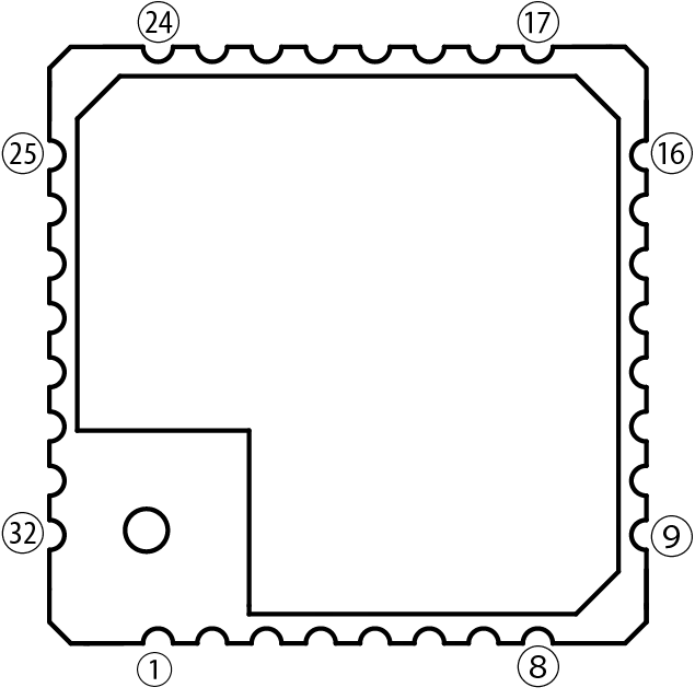
Pin Number Assignment
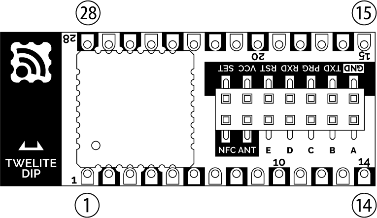
Pin Number Assignment (DIP)
Functions of Each Pin
ALLThe representative functions are shown in the table below.
| Name | Function |
|---|---|
| PIO | Peripheral input/output |
| PWM | Pulse-width modulation output |
| TXD | UART Data Transmission |
| RXD | UART Data Reception |
| RTS | UART Request to Send (output) |
| CTS | UART Clear to Send (input) |
| SCL | I2C Serial Clock |
| SDA | I2C Serial Data |
| SCK | SPI Serial Clock |
| MOSI | SPI Controller Output (PICO) |
| MISO | SPI Controller Input (POCI) |
| SSELN | SPI Peripheral Select (CS) |
| Name | Function |
|---|---|
| IO | Quad SPI Serial Data |
| CSN | Quad SPI Chip Select |
| CLK | Quad SPI Serial Clock |
| MAT | Timer Output |
| CAP | Timer Input |
| OUT | Comparator Output |
| ACP | Comparator + Input |
| ACM | Comparator - Input |
| SWDIO | SWD Serial Data |
| SWO | SWD Trace Port |
| SWCLK | SWD Serial Clock |
| ISPENT | ISP Entry |
| ISPSEL | ISP Mode Select |
The typical function assignments are shown in the following table.
| SMD#Note 1 | DIP# (14P)Note 1 | IONote 2 | PWMNote 3 | ADCNote 3 | UARTNote 3 | I2CNote 3 | SPINote 3 | QuadSPINote 3 | Timer(CT32)Note 3 | ComparatorNote 3 | SWDISPNote 3 |
|---|---|---|---|---|---|---|---|---|---|---|---|
| 1 | 6 | PIO0 | PWM0 | TXD1 | SCK1 | ||||||
| 2 | 7(PRG) | PIO5 | RTS0 | SSELN0MISO1SSELN1(2) | ISPENT | ||||||
| 3 | 5 | PIO2 | PWM2 | RXD0 | SCK0MOSI1 | ||||||
| 4 | 8 | PIO3 | PWM3 | TXD0 | MISO0SSELN1(0) | ||||||
| 5 | 28(VCC) | VCC | |||||||||
| 6 | 9 | PIO7 | PWM7 | CTS0RXD1 | SDA1 | MISO0 | CT32B1MAT1 | ||||
| 7 | 4 | PIO6 | PWM6 | RTS0TXD1 | SCL1 | SCK0 | CT32B1MAT0 | ||||
| 8 | 10(TXD) | PIO8 | PWM8 | TXD0 | MOSI0 | CT32B0MAT0 | OUT | ||||
| 9 | 3(RXD) | PIO9 | PWM9 | RXD0 | SSELN0 | CT32B1CAP1 | |||||
| 10 | 11(A) | PIO14 | PWM1 | ADC0 | SSELN1(1) | CT32B0CAP1 | SWO | ||||
| 11 | 12 | PIO12 | PWM0 | SCL1 | MOSI0 | OUT | SWCLK | ||||
| 12 | 13 | PIO4 | PWM4 | CTS0 | MOSI0SSELN1(1) | ISPSEL | |||||
| 13 | 15(SET) | PIO13 | PWM2 | SDA1 | MOSI0 | SWDIO | |||||
| 14 | 2 | PIO10 | TXD1 | SCL0 | SCK0 | CT32B0CAP0 | |||||
| 15 | 16 | PIO1 | PWM1 | RXD1 | MISO1 | ||||||
| 16 | 17 | PIO0 | PWM0 | TXD1 | SCK1 | ||||||
| 17 | 19 | PIO11 | RXD1 | SDA0 | MISO0 | CT32B1CAP0 | |||||
| 18 | 18 | PIO20 | PWM8 | TXD1 | IO2 | ACP | |||||
| 19 | 20 | PIO21 | PWM9 | IO1 | ACM | SWO | |||||
| 20 | 1,14 | GND | |||||||||
| 21 | 21(RST) | RSTN | |||||||||
| 22 | 24(A) | PIO14 | PWM1 | ADC0 | SSELN1(1) | CT32B0CAP1 | SWO | ||||
| 23 | 22(B) | PIO15 | PWM3 | ADC1 | SCL0 | SCK1 | OUT | ||||
| 24 | 23(C) | PIO16 | PWM5 | ADC2 | SDA0 | SSELN1(0) | CSN | ||||
| 25 | 25(D) | PIO17 | PWM6 | ADC3 | MOSI1 | IO3 | SWO | ||||
| 26 | 26(E) | PIO18 | PWM7 | ADC4 | TXD0 | MISO1 | CLK | CT32B0MAT1 | |||
| 27 | 27 | PIO19 | PWM4 | ADC5 | RXD0RXD1 | IO0 | |||||
| 28 | 1,14(GND) | GND | |||||||||
| 29 | N/A(ANT R) | LA | |||||||||
| 30 | 1,14GND | GND | |||||||||
| 31 | N/A(ANT L) | LB | |||||||||
| 32 | 1,14GND | GND |
Note 1. These are the pin numbers. TWELITE and TWELITE DIP have different counts and assignments. IO names are generally used to identify pins.
Note 2. IO names of the pins. These names are used in semiconductor datasheets and TWELITE application development. Our technical support also refers to pins by IO names in principle.
Note 3. This table lists representative functions. Only a subset is supported in the TWENET library.
To maintain compatibility with TWELITE BLUE/RED series, the following pins are internally connected:
- PIO0: SMD#1 and SMD#16
- PIO14: SMD#10 and SMD#22
It is recommended to connect all GND pins: SMD#28, 30, and 32.
Even if these pins are left unconnected, no significant changes in wireless performance have been observed.
Electrical Characteristics
ALLAbsolute Maximum Ratings
| Min | Max | ||
|---|---|---|---|
| Power Supply | -0.3 | 3.96 | V |
| Reset | -0.3 | 3.96 | V |
| Digital I/O | -0.3 | 3.96 | V |
| ADC | -0.3 | 3.96 | V |
| NFC (LA/LB) | -0.3 | 4.6 | V |
Values are based on the semiconductor datasheet.
Recommended Operating Conditions
| Symbol | Condition | Min | Max | ||
|---|---|---|---|---|---|
| Supply Voltage | VCC | 1.9 | 3.6 | V | |
| Operating Temp | TJ | No condensationMW-G-W | -40 | 105 | °C |
| No condensationMW-G-U | -40 | 90 | °C |
Values are based on the semiconductor datasheet.
DC Characteristics
| Symbol | Condition | Min | Typ | Max | ||
|---|---|---|---|---|---|---|
| Current Cons. | ICC | Sleep, SRAM not retained, no timer | 350 | nA | ||
| Sleep, SRAM not retained, with timer | 800 | nA | ||||
| Sleep, 4KB SRAM retained, with timer | 1025 | nA | ||||
| Sleep, 8KB SRAM retained, with timer | 1120 | nA | ||||
| Active, TX (10dBm) | 20.28 | mA | ||||
| Active, TX (3dBm) | 9.44 | mA | ||||
| Active, TX (0dBm) | 7.36 | mA | ||||
| Active, RX | 4.3 | mA |
Values are based on the semiconductor datasheet.
I/O Characteristics
| Symbol | Condition | Min | Typ | Max | ||
|---|---|---|---|---|---|---|
| PIO Pull-up Resistor | Rpu(int)(PIO) | 40 | 50 | 60 | kΩ | |
| RSTN Pull-up Resistor | Rpu(int)(RSTN) | 40 | 50 | 60 | kΩ | |
| PIO Pull-down Resistor | Rpdn(int)(PIO) | 40 | 50 | 60 | kΩ | |
| IO Input High | VIH | 0.7 * VCC | VCC | V | ||
| IO Input Low | VIL | -0.3 | 0.27 * VCC | V | ||
| IO Output High | VOH | PIO0-9,12-16, 2mA load (VCC=3.6V) | 3.3 | VCC | V | |
| PIO0-9,12-16, 2mA load (VCC=3.0V) | 2.65 | VCC | V | |||
| PIO0-9,12-16, 2mA load (VCC=2.4V) | 2.0 | VCC | V | |||
| PIO0-9,12-16, 2mA load (VCC=1.9V) | 1.4 | VCC | V | |||
| PIO17-21, 5mA load (VCC=3.6V) | 3.2 | VCC | V | |||
| PIO17-21, 5mA load (VCC=3.0V) | 2.6 | VCC | V | |||
| PIO17-21, 5mA load (VCC=2.4V) | 2.05 | VCC | V | |||
| PIO17-21, 5mA load (VCC=1.9V) | 1.35 | VCC | V | |||
| PIO10,11, 2mA load (VCC=3.6V) | 3.3 | VCC | V | |||
| PIO10,11, 2mA load (VCC=3.0V) | 2.66 | VCC | V | |||
| PIO10,11, 2mA load (VCC=2.4V) | 2.1 | VCC | V | |||
| PIO10,11, 2mA load (VCC=1.9V) | 1.15 | VCC | V | |||
| IO Output Low | VOL | 0 | 0.4 | V |
Values are based on the semiconductor datasheet.
ADC Characteristics
| Symbol | Condition | Min | Typ | Max | ||
|---|---|---|---|---|---|---|
| Input Voltage | Vi | 0 | VCC | V | ||
| Full Scale Range | FSR | After calibration | 3.56 | 3.6 | 3.62 | V |
| Resolution | 12 | bits | ||||
| Current Consumption | IADCx | x=05 | 100 | µA | ||
| Integral Non-linearity | INL | 1.1 | LSB | |||
| Differential Non-linearity | DNL | 0.85 | LSB | |||
| Offset Error | EO | After calibration | -4.5 | 4.5 | mV | |
| Gain Error | EG | After calibration | -40 | 0 | 20 | mV |
| Sampling Frequency | fs | Single channel | 78.4 | 100 | 190 | ksps |
Values are based on the semiconductor datasheet.
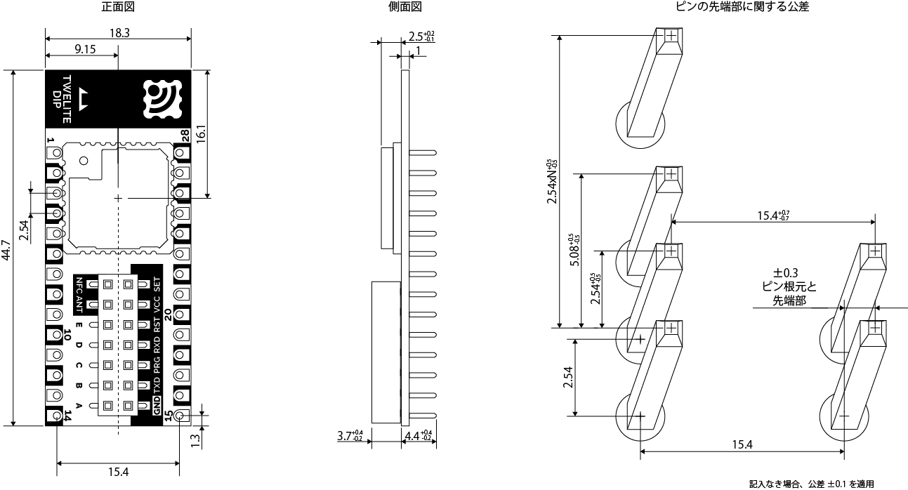
Mechanical Characteristics
External Dimensions
SMD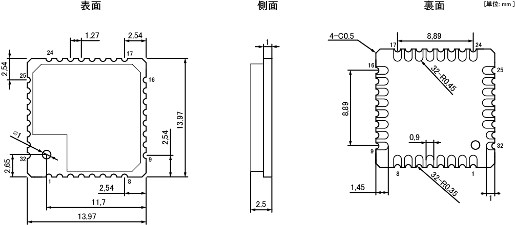
Outline Drawing
- Dimensions: 13.97mm x 13.97 mm x 2.5mm
- Weight: 0.84g (MW-G-W), 0.86g (MW-G-U)
Outline Drawing (PCB Antenna)
Outline Drawing (U.FL)
- Dimensions: 44.7mm x 18.3 mm x 8.1mm
- Weight: 3.81g (MW-G-DIP-P), 3.83g (MW-G-DIP-U)
Recommended Pad Dimensions
SMD
- Do not place silk screen or through-holes on the receiving PCB area that contacts the back of the module.
- When connecting wire antennas such as matchstick antennas, create a rectangular hole in the receiving PCB and solder from the back side. (See Antenna Mounting Opening)
- Use a metal mask thickness in the range of t = 0.12 to 0.15mm. Depending on the metal mask and reflow conditions, solder fillets may not form on some half-holes of the module.
Environmental Regulations
RoHS (10 substances) compliance is planned (note: under analysis).
Shield Can
The shield can is soldered at two diagonal points.
Antenna Mounting Opening
SMDTo connect a matchstick or similar wire antenna when mounting TWELITE on a custom board, create an opening on the board and solder from the back side.
The following figure is one example of such an opening.
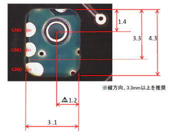
In this example, pins 29, 30, 31, 32 (LA, GND, LB, GND) are left unconnected to allow for a larger opening.
Reflow Conditions
SMDRecommended Reflow Profile
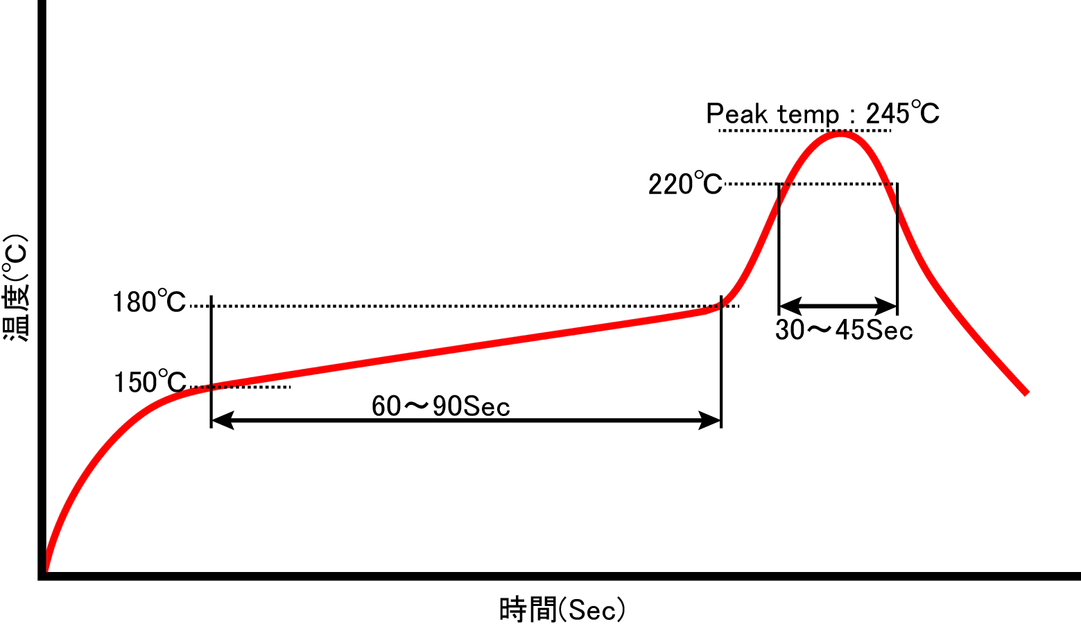
Reflow Profile
| Preheating | Main Heating | Peak Temp | Reflow Count |
|---|---|---|---|
| 150 | 220°C/30-45sec | 245°C | 1 |
Ordering Information
Sales Code
ALL| Product Name | Sales Code | Sales Type | Packaging | MOQ | SPQ |
|---|---|---|---|---|---|
| TWELITE | MW-G-W | Retail | Individual Pack | 1 | 1 |
| MW-G-W-BULK | Wholesale | Cut Tape / Tray | 100 | 100 | |
| MW-G-W-REEL | Wholesale | Reel | 1000 | 1000 | |
| MW-G-U | Retail | Individual Pack | 1 | 1 | |
| MW-G-U-BULK | Wholesale | Cut Tape / Tray | 100 | 100 | |
| MW-G-U-REEL | Wholesale | Reel | 1000 | 1000 | |
| TWELITE DIP | MW-G-DIP-P | Retail | Individual Pack | 1 | 1 |
| MW-G-DIP-P-BULK | Wholesale | Tray | 100 | 100 | |
| MW-G-DIP-U | Retail | Individual Pack | 1 | 1 | |
| MW-G-DIP-U-BULK | Wholesale | Tray | 100 | 100 |
Sales codes are subject to change. Please refer to our website for the latest information.
Packaging
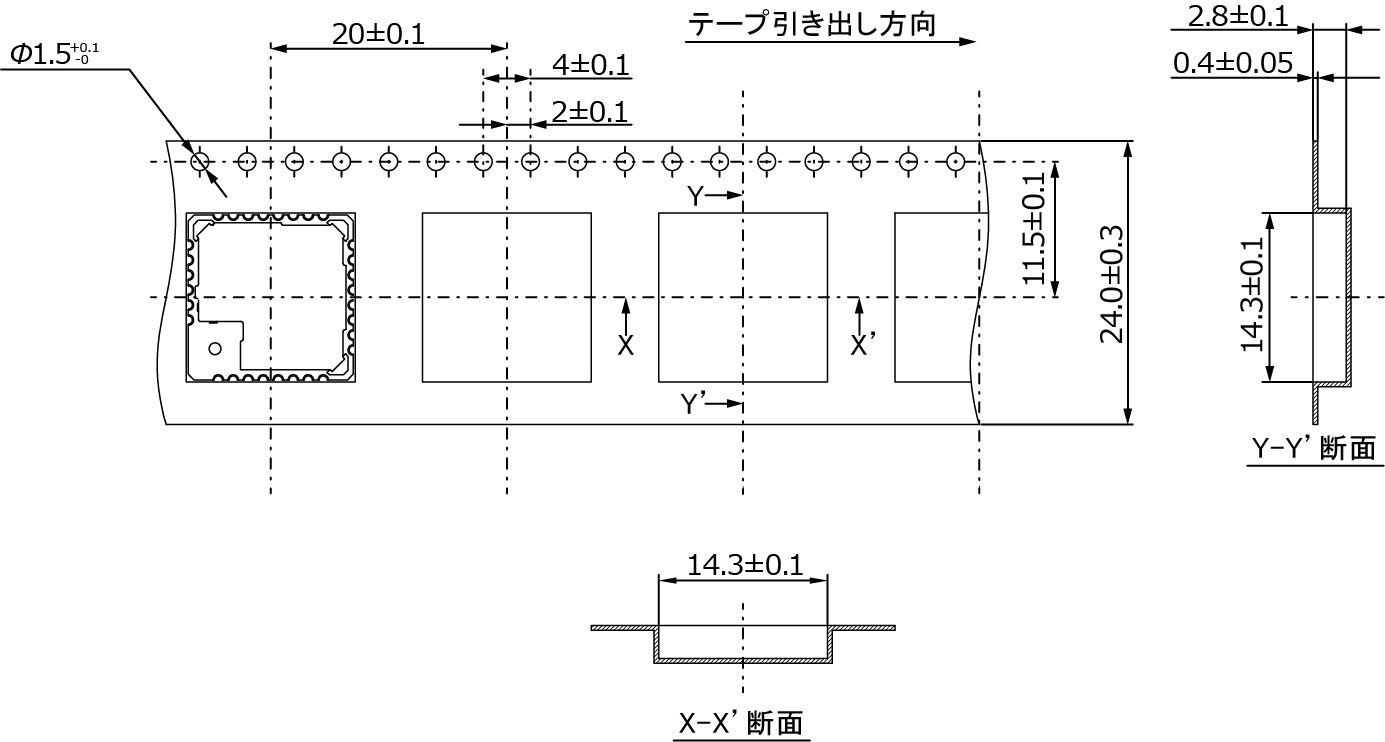
SMDTaping Dimensions
Reel Dimensions

Notes
Mounting Precautions
SMD- The recommended number of reflows is one. During reflow, internal solder may re-melt; handle with care.
- This product is moisture-sensitive. Please perform reflow within 72 hours after opening.
- Use proper anti-static precautions.
- If 72 hours have passed after opening, perform a baking process under the following conditions before use:
- Do not bake in the reel. Transfer to a tray or similar.
- Bake at 90°C for 48 hours, only once.
- Multiple LOT numbers may be mixed in one package.
- Presence or absence of solder fillets on mounted parts is not guaranteed.
- Designed for mounting on FR-4 (glass epoxy). If using a different substrate (e.g., ceramic), evaluate thoroughly beforehand.
- Components mounted inside the product are highly sensitive to static electricity. Ensure sufficient static protection.
- The shield case may come off under stress. Please handle with care.
- For hand soldering, follow these conditions: ≤350°C, ≤3 seconds (≤150°C on package surface).
Export Control
ALL- The AES encryption circuit in TWELITE falls under controlled goods. Contact us for the parameter sheet.
- Depending on the destination, radio certification may be required for customs clearance. Contact us regarding country-specific regulations.
Product Marking
ALLProduct logos and certification numbers printed on the product may change without notice.
Factory Default Firmware
ALLTWELITE (MW-G-W/U, MW-G-DIP-P/U) is shipped with the “Extremely Simple! Standard App (App_Twelite)” pre-installed (at the time of this datasheet’s creation). This app is written during manufacturing to verify chip configuration (e.g., serial number and MAC address), and firmware version information will not be disclosed upon request.
Please note that the presence or type of pre-installed firmware may change without notice. Always write the necessary firmware in your own manufacturing process. We do not provide reflashing services for shipped products.
Storage Precautions
ALLStore at temperatures between 0°C and 40°C, avoiding high temperature and humidity.
SMDUse the product within 6 months of delivery.
Usage Notes
ALLAlways evaluate and verify in your actual usage environment. For high-reliability or life-critical applications, consult your distributor beforehand.
Revision History
| Version | Date | Description |
|---|---|---|
| 1.0.0rc2 | 2024-07-16 | Initial version released |
Arm® and Cortex® are registered trademarks of Arm Limited.
NXP® and NTAG® are registered trademarks of NXP B.V.