Sends input status to parent every 10 seconds, and disables reception to always enter power-saving mode
✅
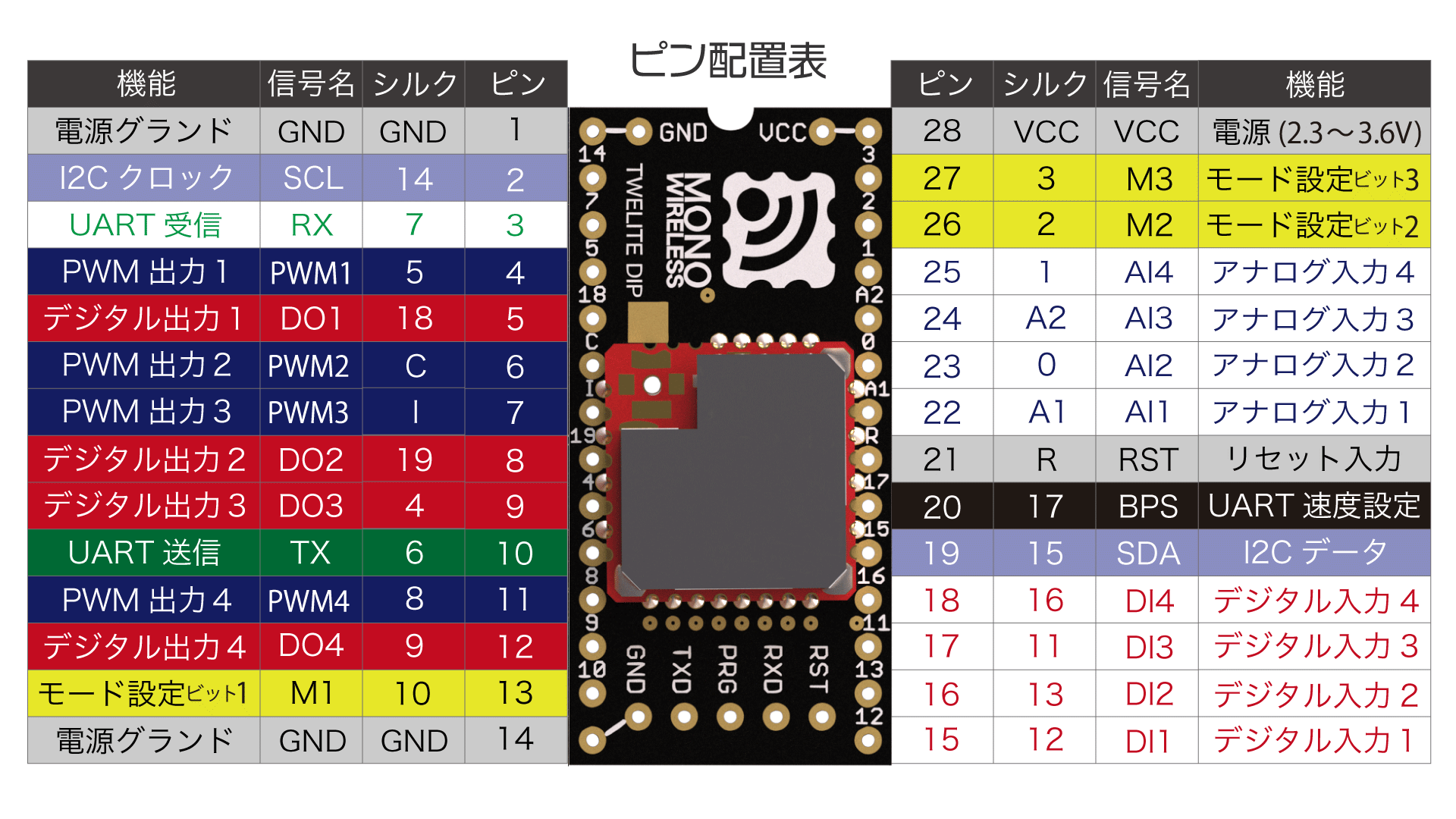
127
O: Not connected (OPEN), G: Connected to GND
Initial state is Child: Continuous mode.
The initial Logical Device ID (LID) used to identify the device varies depending on the mode.
Only in Parent or Repeater modes, the LID can be switched via Interactive Mode.
Please use 121 for Parent and 122 for Repeater.
Handling of unused AIx ports
In Child: Continuous / Child: Continuous 0.03s / Parent: Continuous modes, please connect unused AIx ports to VCC.
Unused AIx ports report undefined values. These modes send data when there is a change in input signals, which may cause unnecessary data transmission.
Parent Device
Continuous Mode
Parent: Continuous Mode
When input signals change or every 1 second, data is sent to all child devices.
It always waits for data sent from child devices, providing good responsiveness but continuously consuming power.
Reception: Always waiting
Transmission: On input change / every 1 second
Disabling periodic transmission
You can disable periodic transmission every 1 second by setting option bit 0x00000002 in Interactive Mode.
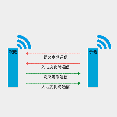
Child Device
Continuous Mode
Child: Continuous Mode
When input signals change or every 1 second, data is sent to all parent devices.
It always waits for data sent from parent devices, providing good responsiveness but continuously consuming power.
Communication image with parent device
Reception: Always waiting
Transmission: On input change / every 1 second
Disabling periodic transmission
You can disable periodic transmission every 1 second by setting option bit 0x00000002 in Interactive Mode.
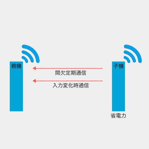
Child: Continuous 0.03s Mode
This mode shortens the periodic transmission interval of Child: Continuous Mode from 1 second to 0.03 seconds.
Although it always waits for data sent from the parent, the communication from child to parent occupies the bandwidth, making the parent’s input response slower. It continuously consumes power.
Communication image with parent device
Reception: Always waiting
Transmission: On input change / every 0.03 seconds
Because a single child occupies most of the bandwidth, please avoid using multiple children simultaneously as much as possible.
Intermittent Mode
Child: Intermittent 1s Mode
When input signals change or every 1 second, power-saving mode is canceled and data is sent to all parent devices.
Reception is disabled, so control from the parent device is not possible. This mode has excellent power-saving performance.
Communication image with parent device
Reception: Disabled
Transmission: On input change / every 1 second
Child: Intermittent 10s Mode
When input signals change or every 10 seconds, power-saving mode is canceled and data is sent to all parent devices.
Reception is disabled, so control from the parent device is not possible. This mode has excellent power-saving performance.
Communication image with parent device
Reception: Disabled
Transmission: On input change / every 10 seconds
Child: Intermittent Reception 1s Mode
When input signals change or every 1 second, power-saving mode is canceled and data is sent to all parent devices.
Reception is also performed every 1 second. It has excellent power-saving performance but is inferior to Child: Intermittent 1s Mode.
Communication image with parent device
Reception: Every 1 second
Transmission: On input change / every 1 second
Because reception is intermittent, the parent device must operate continuously.
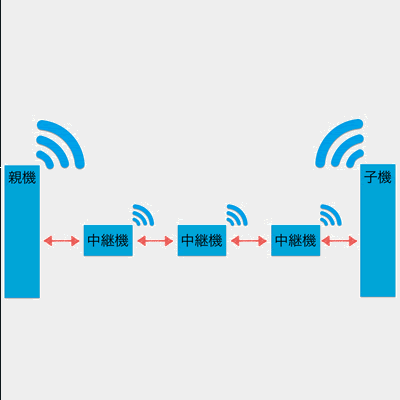
Repeater
Continuous Mode
Repeater: Continuous Mode
The repeater forwards received packets.
Up to three repeaters can be installed between parent and child devices, but increasing repeaters increases the number of packets, which may cause interference.
Image of relaying
Reception: Always waiting
Transmission: On reception
You can also add repeater functionality to child devices. Specify 0x00008000 in the option bits of Interactive Mode.
3 - Alternative Baud Rate Setting for Extremely Simple! Standard App
Changing the baud rate used for UART communication
The Extremely Simple! Standard App (App_Twelite) uses 115200 bps as the default baud rate for UART communication, but this can be changed.
Enabling Alternative Baud Rate Setting
You can enable the alternative baud rate setting by connecting the BPS pin to GND.
The baud rate setting in Interactive Mode indicates the alternative baud rate. If the BPS pin is not connected to GND, the Interactive Mode setting will not be applied.
Interactive Mode uses UART communication. When switching the baud rate of TWELITE, you must adjust the PC side baud rate before using Interactive Mode (Settings in TWELITE STAGE App).
4 - UART Function of Extremely Simple! Standard App
Data format used in UART function
This explains the data format used in the UART function of the Extremely Simple! Standard App (App_Twelite).
Digital and Analog Input/Output
0x81: Status Notification from Remote Device
Outputs the state of the received input signals.
Data Format
#
Data
Content
Note
char
Header
: only
0
uint8
Source Logical Device ID
1
uint8
Command Number
0x81 only
2
uint8
Packet Identifier
Generated from Application ID
3
uint8
Protocol Version
0x01 only
4
uint8
LQI
0-255
5
uint32
Source Serial ID
0x8???????
9
uint8
Destination Logical Device ID
10
uint16
Timestamp
64 counts per second
12
uint8
Relay Count
13
uint16
Power Supply Voltage
Unit is mV
15
int8
-
(Unused)
16
uint8
Digital Signals
Corresponds to DIx from LSB, 0 is High MSB 1 means periodic transmission
Parent 0x00, Child 0-0x7F, All Children 0x78, Self 0xDB
1
uint8
Packet Identifier
0x88 only
2
uint8
Response Number
Number output to response message
3
uint8
Command Number
Write 0x1, Read 0x2, Read/Write 0x4
4
uint8
I2C Address
7-bit
5
uint8
I2C Command
First command byte
6
uint8
Data Size
0 means none
7
[uint8]
Data
Byte sequence of length \(N\)
uint8
Checksum
LRC8
char
Footer
CR (0x0D/'\r')
char
Footer
LF (0x0A/'\n')
For command number 0x4, specify the data size to read and omit the data. The specified I2C command is written, and the specified amount of data is read.
0x89: I2C Output
Data Format
#
Data
Content
Note
char
Header
: only
0
uint8
Source Logical Device ID
Parent 0x00, Child 0-0x7F, All Children 0x78, Self 0xDB
1
uint8
Packet Identifier
0x89 only
2
uint8
Response Number
Number output to response message
3
uint8
Command Number
Write 0x1, Read 0x2, Read/Write 0x4
4
uint8
Result
Failure 0, Success 1
5
uint8
Data Size
0 means none
6
[uint8]
Data
Byte sequence of length \(N\)
uint8
Checksum
LRC8
char
Footer
CR (0x0D/'\r')
char
Footer
LF (0x0A/'\n')
5 - Interactive Mode (Extremely Simple! Standard App)
Detailed configuration changes via Interactive Mode
You can perform detailed configuration of the app via Interactive Mode.
This section explains functions specific to the Extremely Simple! Standard App (App_Twelite). For common features, please refer to the TWELITE APPS manual top page.
Interactive Mode cannot be used while TWELITE is sleeping.
Set the Mx pin settings to Child Continuous Mode or Parent/Relay Mode.
Display Example
The following screen is displayed.
--- CONFIG/TWELITE APP V1-08-2/SID=0x8201001f/LID=0x78 ---
 a: set Application ID (0x67720102)
 i: set Device ID (--)
 c: set Channels (18)
 x: set Tx Power (03)
 t: set mode4 sleep dur (1000ms)
 y: set mode7 sleep dur (10s)
 f: set mode3 fps (32)
 z: set PWM HZ (1000,1000,1000,1000)
 o: set Option Bits (0x00000000)
 b: set UART baud (38400)
 p: set UART parity (N)
---
 S: save Configuration
 R: reset to Defaults
Overrides the intermittent interval of the child intermittent 1-second mode from 1 second to another value. Unit is milliseconds.
Setting 0 disables periodic wakeup by timer. In this case, wakeup occurs on falling edge of DIx but not on rising edge.
y: Child Intermittent 10-second Mode Interval
Overrides the intermittent interval of the child intermittent 10-second mode from 10 seconds to another value. Unit is seconds.
Setting 0 disables periodic wakeup by timer. In this case, wakeup occurs on falling edge of DIx but not on rising edge.
f: Child Continuous 0.03-second Mode Cycle
Overrides the number of transmission requests per second from 32 times to 4/8/16 times. Retry count is not included.
z: PWMx Frequency
If one value is specified, it overrides the frequency of all PWM ports. If specified by comma separation, individual values for PWM1 to PWM4 can be overridden.
o: Option Bits
Specify a 32bit number. Enables settings linked to each bit.
Overrides the alternative baud rate selected when the BPS pin is connected to GND at startup from 38400bps.
Values can be selected from 9600/19200/38400/57600/115200/230400. Specifying other values may cause errors.
This setting is not applied when the BPS pin is left open at startup. The baud rate is fixed at 115200bps.
This is a specification to prevent situations where Interactive Mode becomes unusable due to baud rate changes.
p: UART Parity
N means no parity, O means odd parity, and E means even parity.
Data bits are fixed to 8, stop bits to 1. Hardware flow control cannot be set.
Details of Option Bits
Explanation of settings linked to each bit of the Option Bits value.
00000001: Low Latency Mode
Low Latency Mode shortens the delay on the receiver side by quickly transmitting after detecting changes in DIx.
Low Latency Mode Operation
In the initial state, there is a delay of about 30-70ms until DIx is reflected on DOx. Low Latency Mode shortens this delay to about 3-10ms by simplifying processing to avoid chattering and wireless packet interference.
Falling edge detection uses interrupts
After detection, no new detection occurs for about 100ms
Rising edge detection uses periodic judgment
Transmission occurs if 5 consecutive readings are High at 1ms intervals
(Initially, transmission occurs if 5 consecutive readings are High at 4ms intervals)
No transmission or retransmission delay is set at detection; the wireless packet is immediately sent
Typical delays are about 3-5ms for falling edges and about 10ms for rising edges
Actual delay varies due to transmission/reception failures, etc.
In intermittent mode, the time from wakeup to transmission is also shortened
00000002: Disable Periodic Transmission
Disables periodic transmission every 1 second in continuous mode for child devices.
00000004: Disable Periodic Transmission and UART Output
For child devices: disables periodic transmission every 1 second in continuous mode and stops UART output of received data.
00000010: Disable Transmission on AIx Change
For child devices: disables transmission when AIx input changes in continuous mode.
Since released AIx ports report undefined values, connect them to VCC when analog input is not used. This option allows omission of connection to VCC.
00000020: Disable AIx Value
Sends packets treating unused ports as 0xFFFF without using ADC measurement values.
00000040: Change PWMx Calculation Formula
By default, adjusted output for volume control is applied to PWMx.
This option disables that and outputs full scale for inputs below 1.8V.
Duty Cycle Calculation Formula
Duty cycle \(duty\) can be expressed using input voltage \(V_{input}\) and power supply voltage \(V_{cc}\) as in (1).