This is the multi-page printable view of this section. Click here to print...
Hardware Development
1 - On Power Saving Performance
To achieve low power consumption as a wireless microcontroller module for connecting things, it is necessary to suppress the current consumption of each process, but it is also very important to shorten the startup time and processing time. Even if the current consumption is low, low power consumption cannot be achieved if the processing time is long.
Power Consumption (Current)
The following are typical current consumptions when sending one packet of 30 bytes.
- Standard output BLUE
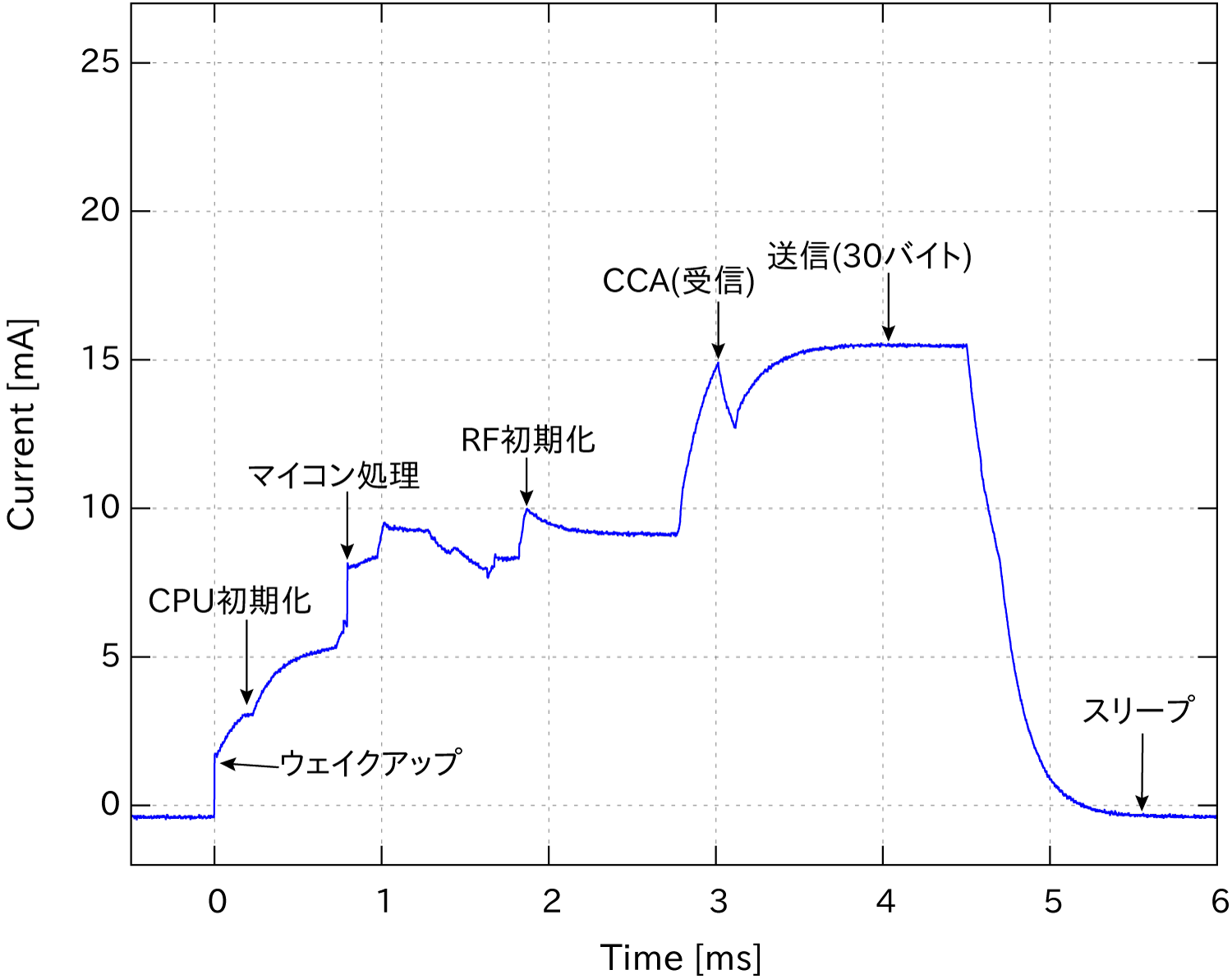
In the case of TWELITE BLUE
- High output RED
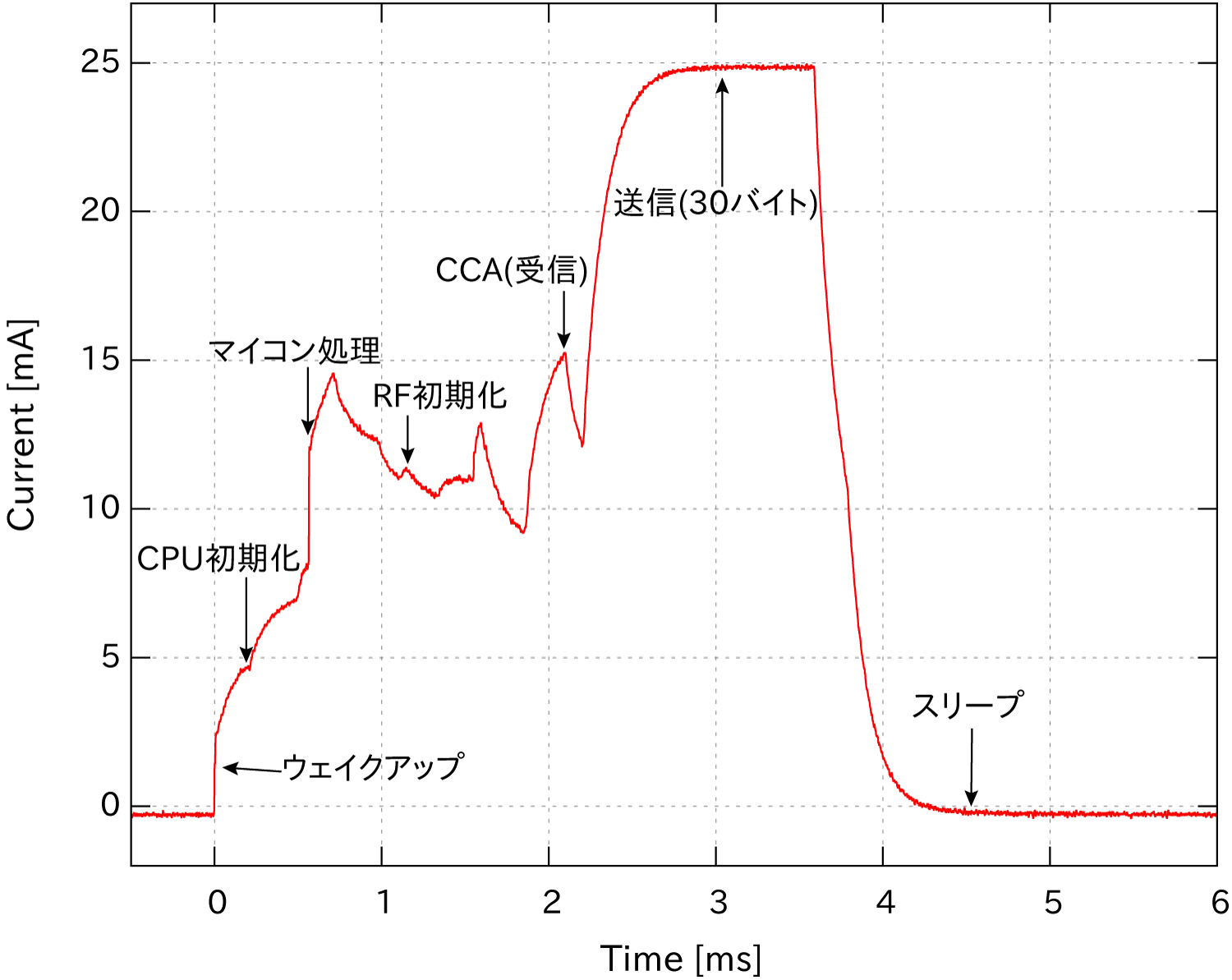
In the case of TWELITE RED
High output RED has a higher current consumption during transmission compared to standard output BLUE, but since the processing time is shorter, the current consumption for sending one packet is equivalent.
TWELITE achieves power saving through low current consumption, instant startup, and high-speed processing.
17.0mA and RED 14.7mA. If continuous reception is required, constant power supply or a battery with large capacity is necessary.Examples of Power Consumption
Here is an example of a wireless tag with minimized power consumption of TWELITE. In this example, no sensors are used, and 4 bytes of ID data are periodically sent using the built-in timer. No reception acknowledgment (ACK) from the transmission counterpart is performed. The average current consumption when sending one packet is 11.6mA, and the processing time is 2.5ms.
- Average current consumption considering only the awake time
11.6[mA] * (2.5/1000)[ms] = 29[uA]
- Average current consumption including sleep (RAM on) time
29[uA] + 1.5[uA] = 30.5[uA] = 0.0305[mA]
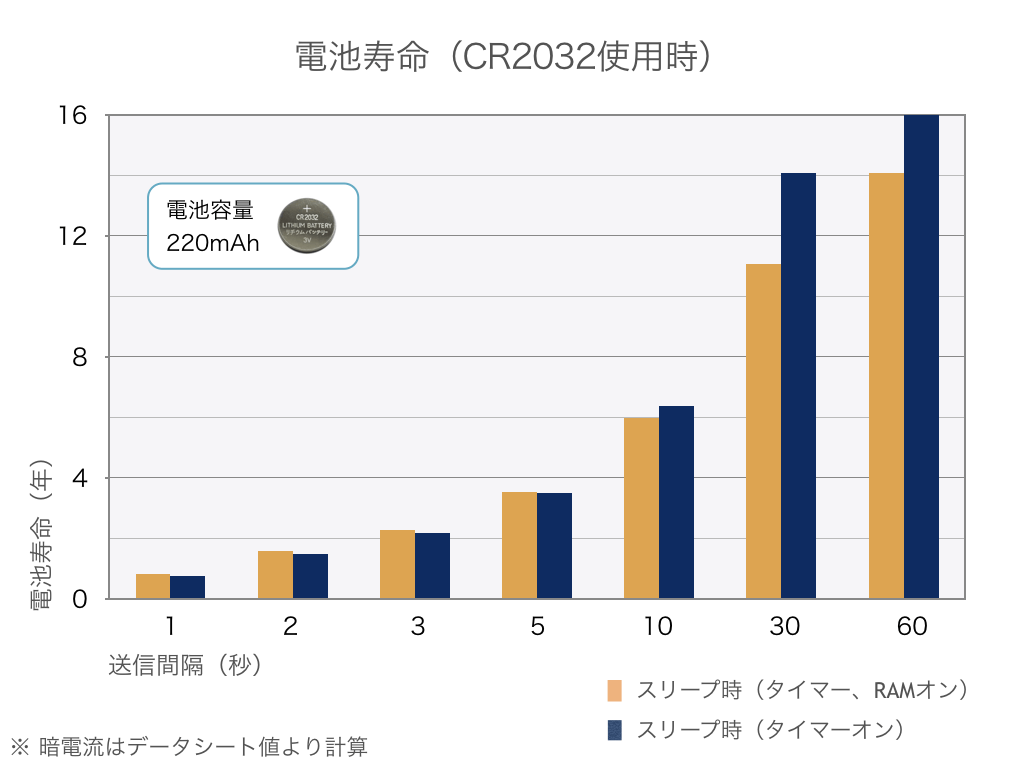
Assuming transmission once every second and a CR2032 battery capacity of 220mAh,
220/( 0.0305 ) = approximately 7213[hours] = 300[days] = 10 months
The graph below shows the battery life when using a coin-type battery (CR2032). The battery life exceeds 10 years when data is sent every 30 seconds.
1.1 - Battery Operation and Buffer Capacitor
When using a small-capacity battery, it may not be able to supply sufficient current. For example, the rated current of a CR2032 is about 0.2mA, and even at maximum, only around 2~3mA is expected.
For instance, when TWELITE transmits a wireless packet, it momentarily consumes about 20mA. At this time, insufficient current supply and voltage drop may occur, causing the system to malfunction.
To avoid this, a buffer capacitor is connected between VCC and GND. (Additionally, it is necessary to control startup using a reset IC.)
Assuming the power is cut off, with a voltage of 3.3V and an average current of 10mA, a 100uF buffer capacitor can keep the system running for about 10ms. From the moment the power is cut off, current is supplied from the buffer capacitor, and the wireless module will operate until the voltage drops near 2V, where the wireless module becomes inoperable.
This is an effective measure for intermittent operation and transmission. A caution is that if retransmissions occur, the time until transmission completion significantly increases. Since one retransmission consumes several milliseconds, a buffer capacitor considering the number of retransmissions is necessary.
However, in cases where the device waits for reception, it continuously consumes a large current (17.2mA), so dealing with this using the above buffer method is difficult. Please use a battery with a higher supply capacity.
Approximate Capacitor Capacity and Operating Time
The current consumption of TWELITE series modules does not depend on the supply voltage. Because the current is constant, we calculate how long the module can operate based on the capacitor’s charge.
If a capacitor with capacitance C stores charge corresponding to voltage v, the time t for the voltage to drop from v to 0 at a constant current i is t = Cv/i.
The time required for the voltage to drop from 3.3V to 2.1V at current i is C(3.3-2.1)/i. For i=10mA and C=100uF, this calculates to 12ms. According to this calculation, if the power to a module operating at 3.3V is suddenly cut, and the average current is 10mA, the operation time can be extended by about 12ms.
The current value of
10mAis only an assumed average. Please refer to actual measured consumption current values.
2 - Antenna Implementation
This document describes important points regarding certification compliance for customer-designed wireless circuits and antennas.
- When certification is obtained by our company and design information is provided to the customer
- Please perform design and production according to the technical information submitted by our company at the time of certification.
- Our certified business partner has been provided with technical information about the RF circuits and antennas. We will present the customer with essential requirements for certification and comments related to performance based on this technical information.
- There may be differences of opinion between the certified business partner and other views. In the unlikely event that problems arise due to these differing opinions, our company and the certified business partner will provide information based on the technical information at the time of certification, but the following actions will not be taken:
- Conducting negotiations or equivalent actions.
- Compensation arising from these issues.
- For overseas certification, please verify compliance status by yourself.
- Requirements for overseas certification may be updated. Please refer to the latest information at that time.
- We cannot provide a final opinion on the appropriateness of your design and implementation.
- When the customer designs independently
- In most cases, certification is required for independent designs.
- To facilitate smooth handling of technical documents related to certification, we generally guide you to our designated business partners. Please contact us for details.
2.1 - Implementation of Inverted-F Antenna
This document describes important notes regarding the radio certification of the inverted-F pattern antenna (TWELITE-SMD-ANT-REVF).
The reference design is published at the following link.
monowireless/PCB_REF_DESIGN_KICAD: Reference Schematic/PCB design data for KiCAD
Requirements
The following conditions must be satisfied.
- Wiring must be done according to the pattern and through-holes as per the design data.
- Do not modify areas marked as no-change (DO NOT WIRE) in the design data.
- The specified printed circuit board must be used.
- Please specify a 1mm thickness to the PCB manufacturer.
- (If a thickness other than 1mm is required, please refer to the notes below.)
- Due to dielectric properties, glass epoxy (FR-4) must be specified. Other materials are not allowed.
- Layer structure must be double-sided or 4-layer.
- There are no specific requirements for solder mask color or silkscreen.
- Confirm that manufacturing and assembly are performed as per the design.
- There should be no design deviations exceeding commonly accepted tolerances.
- The wireless module must be properly mounted.
Design and Performance
GND Area
The inverted-F antenna consists of an inverted-F shaped element and a GND pattern directly beneath the module. The area of the GND pattern significantly affects performance. The optimal size is between 20x20 mm and 40x40 mm.
Wiring
The inverted-F antenna is sensitive to external wiring. For example, wireless tags such as TWELITE CUE that place a coin cell holder on the GND surface without external wiring can achieve near-ideal performance.
If some wiring must be routed on the GND surface, keep it to a minimum. For example, having just one wire passing through generally has negligible impact.
Performance Evaluation
Certification Status
Japan
Applicable Modules
- TWE-L-WX
- MW-R-WX
Requirements
Must satisfy the above requirements.
North America (FCC)
Please ensure compliance yourself regarding overseas certifications.
Applicable Modules
- TWE-L-WX
Requirements
- Must satisfy the above requirements.
- Other requirements such as labeling should follow FCC rules.
Europe (EU)
Please ensure compliance yourself regarding overseas certifications.
Applicable Modules
- TWE-L-WX
Requirements
- Must satisfy the above requirements.
- Other requirements such as labeling should follow CE rules.
Other Regions
No certification support.
About PCB Thickness
This design specifies an FR-4 1mm thick PCB. This thickness is the basis for radio certification approval, so using a different thickness will result in loss of certification.
However, for Japan domestic certification only, the following PCB thicknesses are also approved:
- t=0.5mm (Not approved for overseas certifications obtained by us)
- t=0.8mm (Not approved for overseas certifications obtained by us)
- t=1.6mm (Not approved for overseas certifications obtained by us)
Since the antenna pattern is optimized for t=1mm, characteristics will slightly change. However, the change is usually very minor. Characteristic patterns on PCBs sized according to the ideal GND size show changes of about 1 to 3 dB.
2.2 - Implementation of SMA Connector
This document provides important notes regarding the radio certification of the SMA connector (TWELITE-SMD-SMA-CONN).
The reference design is published at the following location.
monowireless/PCB_REF_DESIGN_KICAD: Reference Schematic/PCB design data for KiCAD
Requirements
Common
- Wire according to the pattern and through-holes as specified in the design data
- Do not modify areas marked as “No wiring, DO NOT WIRE” in the design data
- Use the specified printed circuit board
- Specify a thickness of 1mm to the PCB manufacturer
- Due to dielectric constant considerations, use glass epoxy (FR-4); other materials are not allowed
- Layer structure should be double-sided or 4-layer
- There are no specific requirements for solder resist color or silk screen
- Confirm that manufacturing and assembly are according to the design
- Ensure no design deviations exceed commonly cited tolerances
- Confirm that the wireless module is properly mounted
- Use the specified connector
Specified Connector
TOCONNE SMA-LR4 (Au)
COSMTEC RESOURCES S-037-TGG
https://akizukidenshi.com/catalog/g/gC-02569/
Available at Akizuki Denshi Tsusho
Certification Status
Japan
Target Modules
- TWE-L-WX
- MW-R-WX
Requirements
- Must satisfy the above requirements
North America (FCC)
No certification support.
Europe (EU)
No certification support.
Other Regions
No certification support.
2.3 - Implementation of Wire Antenna
You can create an antenna using a wire with a diameter of φ=0.8mm or less.
It can be bent arbitrarily for use, but performance may significantly decrease compared to when it is upright. To maintain antenna performance, please refer to “Wire Antenna Bending Patterns.” (Keep dimensional differences within 0.5mm.)